2GM
2-3-23
Connector Pin No. Signal I/O Description
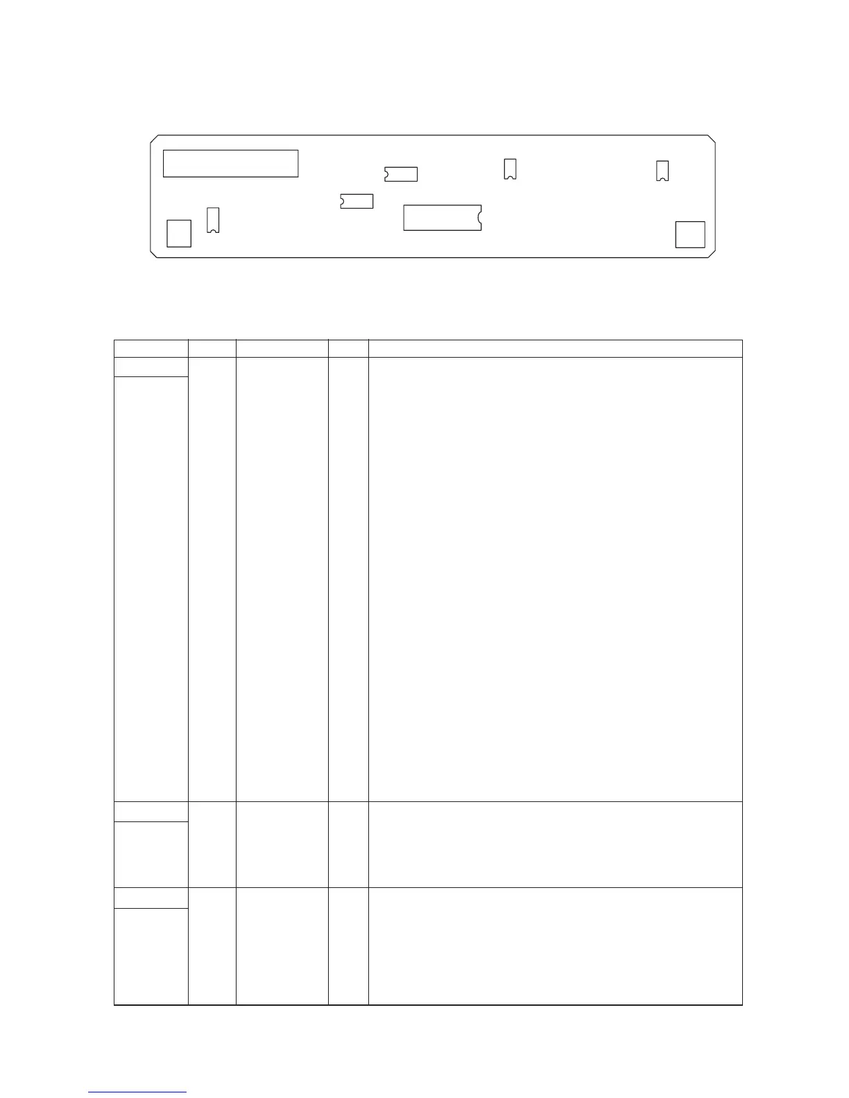
Figure 2-3-17 CCD PWB silk-screen diagram
YC1
1
1
13
2
30
YC2
YC3
U7
U6
U4
U9
U8
U3
YC1
Connected
to the
scanner
PWB
YC2
Connected
to the
inverter
PWB
YC3
Connected
to the
scanner
home
position
sensor
1 GND - Ground
2 GND - Ground
3 GND - Ground
4 SW I Color/monochro control signal
5 SWN I Color/monochro control signal
6 SH I CCD shift signal
7 GND - Ground
8 CPN I CCD CP signal
9 GND - Ground
10 RSN I CCD RS signal
11 GND - Ground
12 CCDCLK I CCD clock signal
13 GND - Ground
14 CCDCLKN I CCD clock signal
15 GND - Ground
16 GND - Ground
17 GND - Ground
18 CCDG(O) O Image data G (green) signal (analog)
19 GND - Ground
20 CCDB(E) O Image data B (blue) signal (analog)
21 GND - Ground
22 CCDR O Image data R (red) signal (analog)
23 +12 V I 12 V DC power supply
24 +5 V I 5 V DC power supply
25 +5 V I 5 V DC power supply
26 HPSWN O Scanner home position sensor: On/Off
27 PGND - Ground
28 PGND - Ground
29 LAMP I Exposure lamp: On/Off
30 LAMP I Exposure lamp: On/Off
1 LAMP O Exposure lamp: On/Off
2 PGND - Ground
1 GND - Ground
2 HPSWN I Scanner home position sensor: On/Off
3 +5 V O 5 V DC power supply