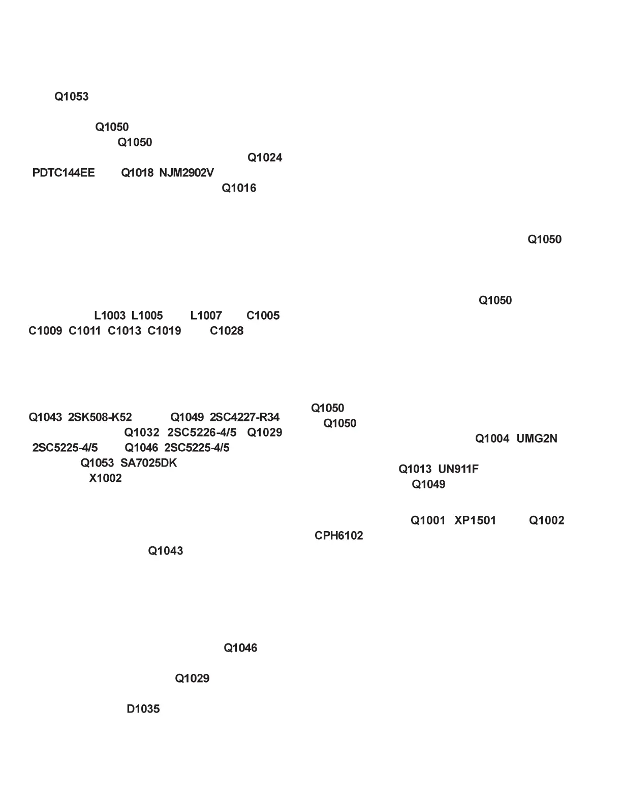
16
Transmit Inhibit
When the Transmit PLL is unlocked, pin 18 of PLL
chip
goes to logic "low." The resulting DC
“unlock“ control voltage is passed to pin 20 of mi-
croprocessor
. While the transmit PLL is un-
locked, pin 85 of
remains low, which then
turns off the Automatic Power Controller
( ) and ( ) to disable the
supply voltage to the Power Module
, dis-
abling the transmitter.
Spurious Suppression
Generation of spurious products by the transmitter
is minimized by the fundamental carrier frequency
being equal to final transmitting frequency, modu-
lated directly in the transmit VCO. Additional har-
monic suppression is provided by a low-pass filter
consisting of
, , and and ,
, , , , and , result-
ing in more than 60 dB of harmonic suppression prior
to delivery of the signal to the antenna.
PLL Frequency Synthesizer
The PLL frequency synthesizer consists of the VCO,
( : RX) or ( :
TX); VCO buffers
( ),
( ) and ( ); PLL sub-
system IC
( ) and 14.6 MHz refer-
ence crystal
.
The frequency stability is ±2.5 ppm within the tem-
perature range of -30° to +60°C. The output of the
14.6 MHz reference is applied to pin 8 of the PLL IC.
While receiving, VCO
oscillates between
355.75 and 467.75 MHz according to the transceiver
version and the programmed receiving frequency.
The VCO generates at 355.75 to 467.75 MHz for pro-
viding to the first local signal. In the transmit mode,
the VCO generates 400 to 512 MHz.
The output of the VCO is amplified by
, and
is routed to pin 5 of the PLL IC. Also the output of
the VCO is amplified by the
and routed to
the first local and the drive chain according
toinstructions from
.
The PLL IC consists of a prescaler, fractional divider,
reference divider, phase comparator, and a charge
pump. This PLL IC is a fractional-N type synthesizer
utilizing a 40 or 50 kHz reference signal which is
eighth multiple of the channel step size (5, 6.25 or
7.5 kHz). The input signal from pins 5 and 8 of the
PLL IC is divided down to 40 or 50 kHz and com-
pared at the phase comparator. The pulsed output
signal of the phase comparator is applied to the
charge pump and transformed into a DC signal in
the loop filter. The DC signal is applied to the pin 1
of the VCO and locks to keep the VCO frequency
constant.
PLL data is delivered from DTA (pin 100), CLK (pin
2) and PSTB (pin 98) of the microprocessor
.
The data are applied to the PLL IC when the channel
is changed or when transmission switches is changed
to reception (and vice versa). A PLL lock condition is
always monitored by the pin 20 of
. When the
PLL is unlocked, the "UL" line goes low.
Miscellaneous Circuits
Push-To-Talk Transmit Activation
The PTT switch on the microphone is connected to
pin 32 of microprocessor
, so that when the PTT switch is closed, pin 85
of
goes high. This signals the microprocessor
to activate the TX/RX controller
( ),
which then disables the receiver by interrupting the
5 V supply bus at
( ) to the front-end,
FM IF subsystem IC
, and the receivers VCO
circuitry.
At the same time, ( ) and
( ) activate the TX 5V supply line to enable
the transmitter.
Circuit Description
 Loading...