Manual VIPA System 200V Chapter 3 Analog output modules
HB97E - SM-AIO - Rev. 12/32 3-17
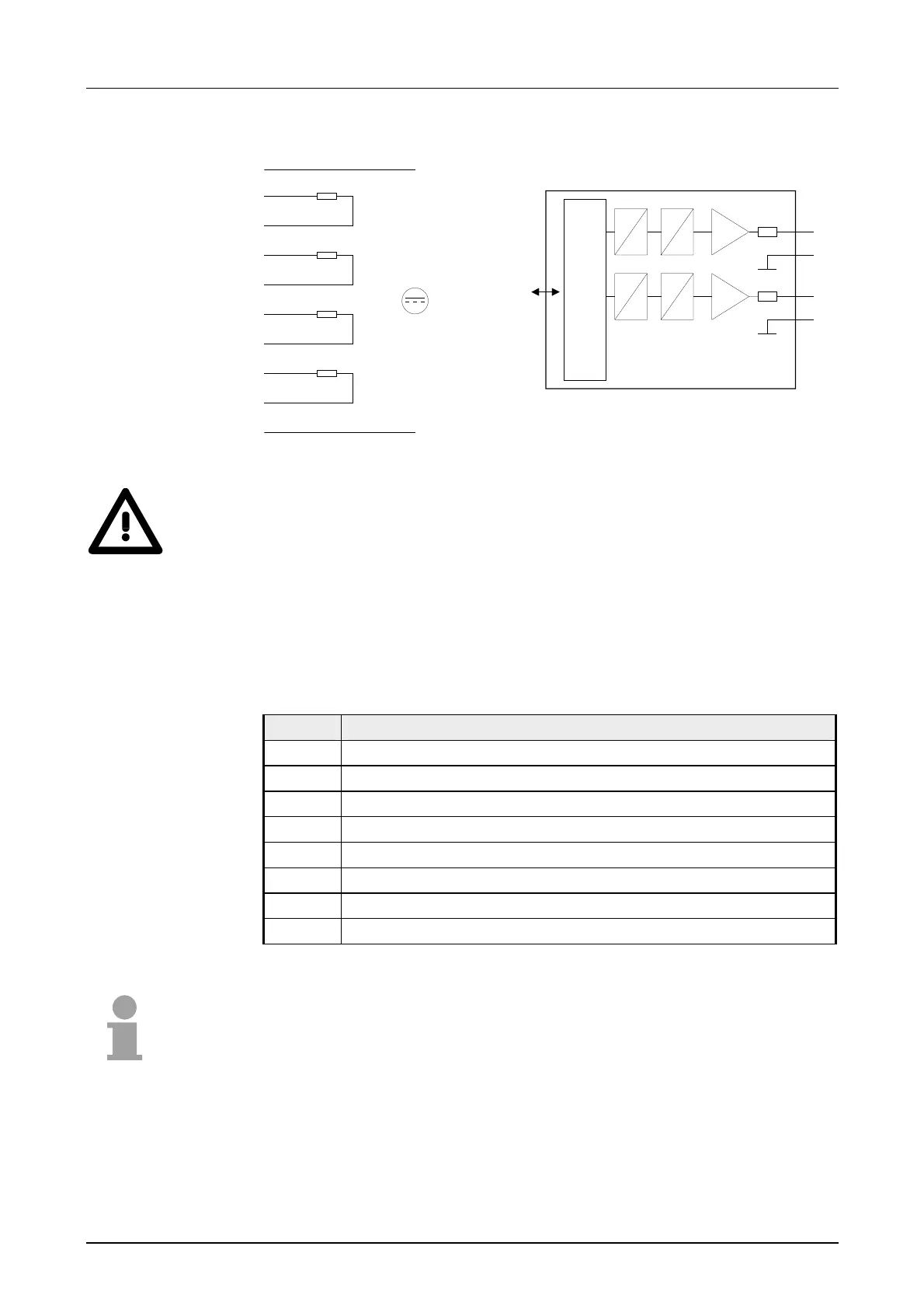
Wiring diagram Schematic diagram
DC 24
1
2
3
4
5
6
7
8
9
10
L+
M
V-Bus
Ausgabe
µP
Kanal 0
+0
M0
Kanal 1
+1
M1
.
.
.
D
A
D
A
Attention!
Switching off and on the load nominal voltage (L+) could lead to wrong
values on the output for ca. 80ms!
The value of the output data is entered into the data output area. For every
channel you may configure the relationship between the output value and
the respective current or voltage by means of a function-no..
The following table shows the structure of the data output area:
Data output area:
Byte Bit 7 ... Bit 0
0 High-Byte channel 0
1 Low-Byte channel 0
2 High-Byte channel 1
3 Low-Byte channel 1
4 High-Byte channel 2
5 Low-Byte channel 2
6 High-Byte channel 3
7 Low-Byte channel 3
Note!
When new values are transferred from the CPU to the module, the module
needs one cycle to update all outputs abbr. if the analog values change
within this cycle, these are at least available at the concerning outputs at
the end of the next following cycle.
Wiring and
schematic
diagram
Data output