32 www.xilinx.com AC701 Evaluation Board
UG952 (v1.3) April 7, 2015
Chapter 1: AC701 Evaluation Board Features
GTP Transceiver Clock Multiplexer Input Clock Sources
This section describes the GTP 213 Multiplexer U3 and U4 input clock circuits as listed in
Table 1-11.
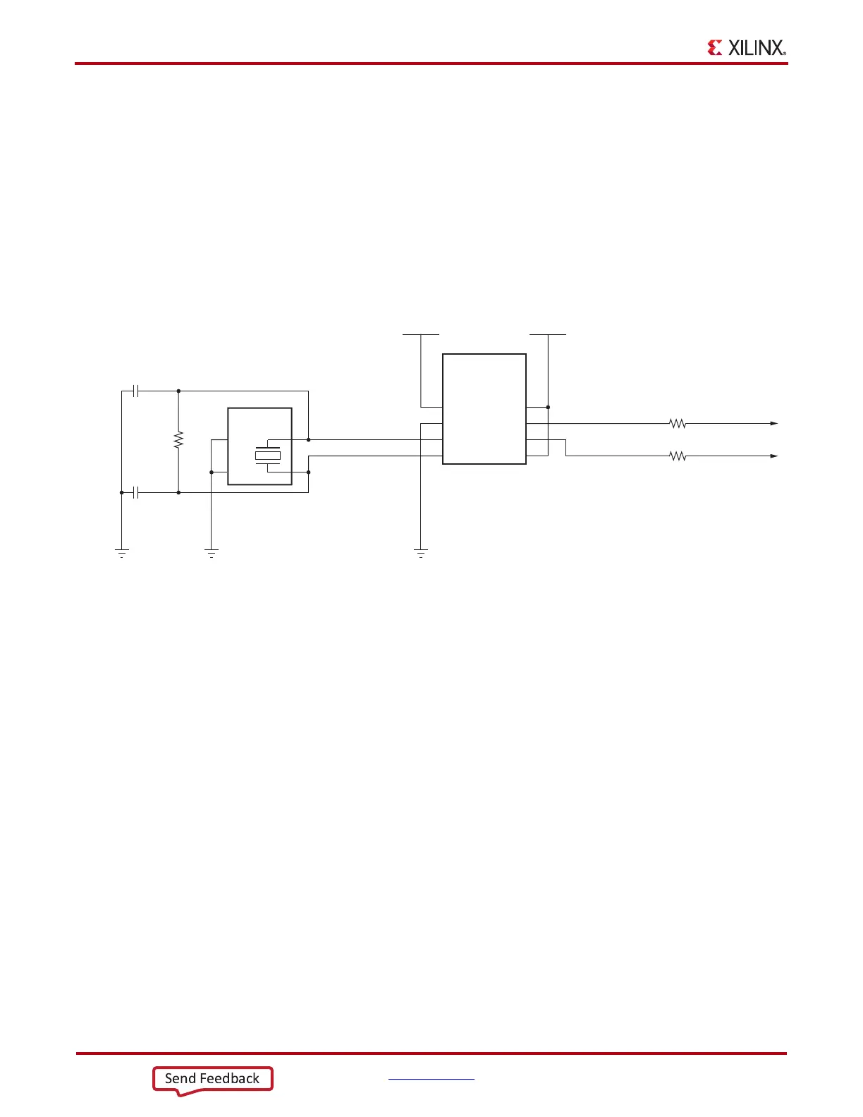
U3 IN0: 125 MHz Clock Generator
[Figure 1-2, callout 15]
Clock Multiplexer U3 IN 0 (pin 4 P, pin 2 N) is driven by U2 ICS84402I Crystal-to-LVDS
clock generator. This device uses 25
MHz crystal X3 as its base input frequency and, using
an internal VCO, multiplies this by five to produce a 0.45
ps (typical) RMS phase jitter,
125
MHz LVDS output. The circuit for the 125 MHz clock is shown in Figure 1-17.
X-Ref Target - Figure 1-17
Figure 1-17: AC701 Board 125 MHz U3 MUX IN0 Source Circuit
GND_EPHYCLK GND_EPHYCLKGND_EPHYCLK
R320
1.0M 5%
R487
0Ω 5%
R486
0Ω 5%
C300
18pF 50V
NPO
C301
18pF 50V
NPO
EPHYCLK_XTAL_OUT
GND2
GND1
X2
X1
X3
25.00 MHz
50 ppm
EPHYCLK_XTAL_IN
2
1
3
4
VDD
Q0
NQ0
OE
XTAL_OUT
XTAL_IN
GND
VDDA
8
7
6
5
3
4
2
1
U2
VDDA_EPHYCLK
EPHYCLK_Q0_C_N EPHYCLK_Q0_N
EPHYCLK_Q0_C_P EPHYCLK_Q0_P
ICS844021I
VDD_EPHYCLK
UG952_c1_13_101512