AC701 Evaluation Board www.xilinx.com 33
UG952 (v1.3) April 7, 2015
Feature Descriptions
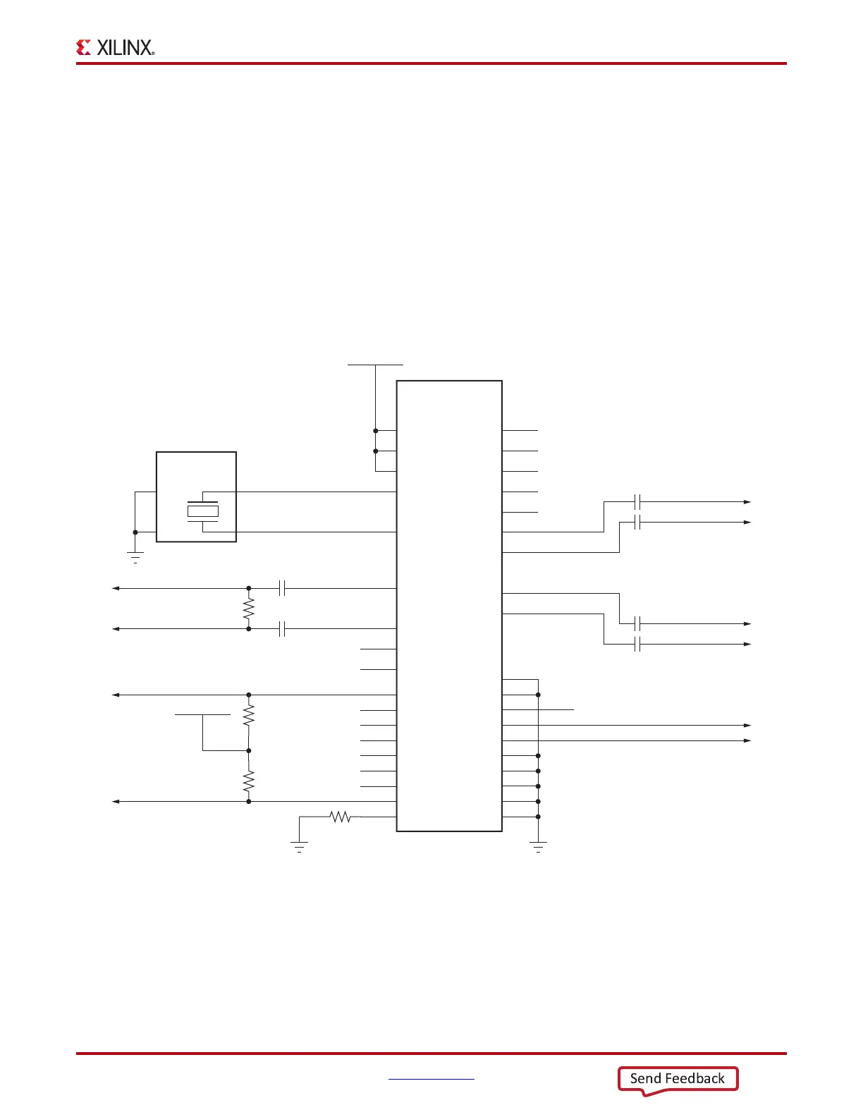
U3/U4 IN1: Jitter Attenuated Clock
[Figure 1-2, callout 10]
The AC701 board includes a Silicon Labs Si5324 jitter attenuator U24 on the back side of the
board. FPGA user logic can implement a clock recovery circuit and then output this clock
to a differential I/O pair on I/O bank 16 (REC_CLOCK_C_P, FPGA U1 pin D23 and
REC_CLOCK_C_N, FPGA U1 pin D24) for jitter attenuation. Duplicate capacitively
coupled jitter attenuated clocks are routed to a pair of GTP clock MUX components U3 and
U4. See
Table 1-9, page 27.
The primary purpose of this clock is to support CPRI/OBSAI applications that perform
clock recovery from a user-supplied SFP/SFP+ module and use the jitter attenuated
recovered clock to drive the reference clock inputs of a GTP transceiver. The jitter
attenuated clock circuit is shown in
Figure 1-18.
See the Silicon Labs Si5324 data sheet for more information on this device [Ref 21]. The
SI5324 U24 connections to FPGA U1 are shown in Table 1-10.
X-Ref Target - Figure 1-18
Figure 1-18: Jitter Attenuated Clock
UG952_c1_15_011813
R424
4.7KΩ 5%
SI5324_VCC
SI5324_VCC
Si5324C-C-GM
Clock Multiplier/
Jitter Attenuator
VDDA
GND
XB
XA
NC5
32
6
5
29
28
U24
CKOUT1_N
7
8
CKOUT1_P
C31
0.1μF 25V
X5R
C32
0.1μF 25V
X5R
SI5324_XTAL_XA
GND2
GND1
XB
XA
X6
114.285 MHz
20 ppm
SI5324_OUT0_C_N
SI5324_OUT0_C_P
C9
0.1μF 25V
X5R
C10
0.1μF 25V
X5R
SI5324_OUT1_C_P
SI5324_OUT1_C_N
SI5324_OUT_N
SI5324_OUT_N
SI5324_OUT_P
SI5324_OUT_P
SI5324_XTAL_XB
GND
NC4
2
1
3
4
C33
0.1μF 25V
X5R
C34
0.1μF 25V
X5R
REC_CLOCK_P
REC_CLOCK_N
REC_CLOCK_C_P
REC_CLOCK_C_N
16
17
R167
100Ω
R4
4.7K
R292
4.7K
CKIN1_P
CKIN1_N
NC
NC
12
13
CKIN2_P
CKIN2_N
10
5
VDDA
VDDA
2
NC3
2
NC2
2
NC1
NC
NC
NC
NC
NC
35
34
CKOUT2_N
CKOUT2_P
SI5324_INT_ALM_B 3
NC 4
NC 11
NC 15
NC 18
NC 19
NC 20
SI5326_RST_B 1
21
31
GND2
9
GND1
31
A2_SS
31
A1
24
A0
22
SI5324_SCL
SCL
23
SI5324_SDA
SDA_SDO
27
NC
SDI
36
CMODE
GND
INC
DEC
LOL
RATE1
RATE0
C2B
INT_C1B
CS_CA
RST_B
37
GNDPAD