ML505/ML506/ML507 Evaluation Platform www.xilinx.com 17
UG347 (v3.1.1) October 7, 2009
Detailed Description
R
1. Virtex-5 FPGA
A Xilinx Virtex-5 FPGA is installed on the board. See Appendix A, “Board Revisions” for
device details.
Configuration
The board supports configuration in all modes: JTAG, Master Serial, Slave Serial, Master
SelectMAP, Slave SelectMAP, Byte-wide Peripheral Interface (BPI) Up, BPI Down, and SPI
modes. See the “Configuration Options,” page 53 section for more information.
I/O Voltage Rails
Table 1-1 summarizes the FPGA I/O voltage rail and the voltages applied to each bank.
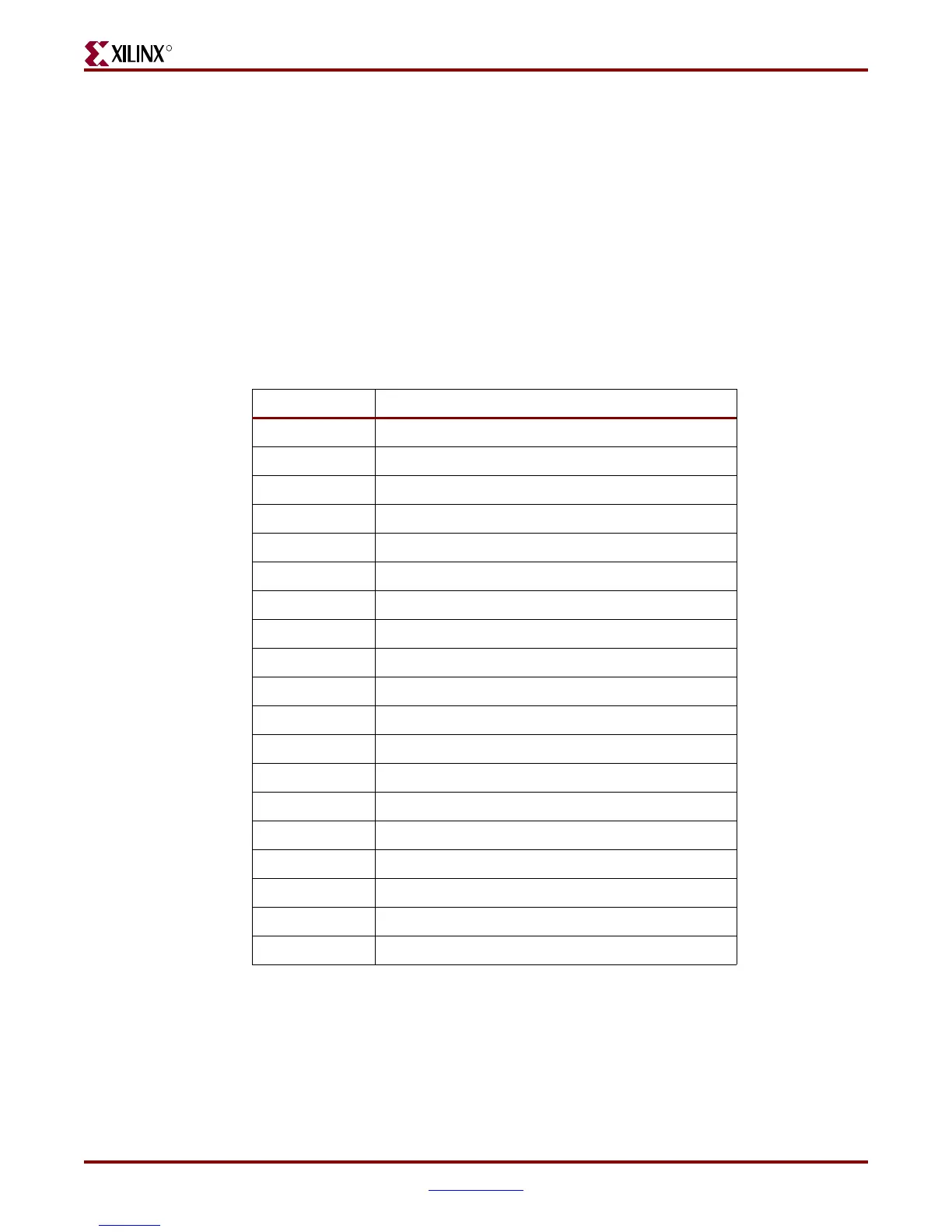
Table 1-1: I/O Voltage Rail of FPGA Banks
FPGA Bank I/O Voltage Rail
03.3V
13.3V
23.3V
32.5V no DCI
43.3V no DCI
5
(1)
3.3V DCI with 49.9Ω resistors installed
63.3V (unused)
11 User selectable as 2.5V or 3.3V using jumper J20
12 3.3V DCI with 49.9Ω resistors installed
13 User selectable as 2.5V or 3.3V using jumper J20
15 1.8V DCI with 49.9Ω resistors installed
17 1.8V DCI with 49.9Ω resistors installed
18 3.3V no DCI
19 1.8V DCI with 49.9Ω resistors installed
20 3.3V DCI with 49.9Ω resistors installed
21 1.8V DCI with 49.9Ω resistors installed
22 3.3V DCI with 49.9Ω resistors installed
23
(1)
3.3V DCI with 49.9Ω resistors installed
25 3.3V (unused)
Notes:
1. Banks 5 and 23 are available on the ML507 only.
Downloaded from Elcodis.com electronic components distributor