ML505/ML506/ML507 Evaluation Platform www.xilinx.com 41
UG347 (v3.1.1) October 7, 2009
Detailed Description
R
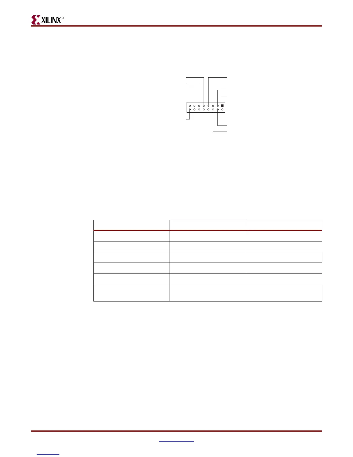
CPU JTAG Header Pinout
Figure 1-8 shows J12, the 16-pin header that can be used to debug the software operating in
the CPU with debug tools such as Parallel Cable IV or third party tools.
CPU JTAG Connection to FPGA
The connections between the CPU JTAG header (J12) and the FPGA are shown in
Table 1-22. These are attached to the PowerPC® 440 processor JTAG debug resources
using normal FPGA routing resources. The JTAG debug resources are not hard-wired to
particular pins and are available for attachment in the FPGA fabric, making it possible to
route these signals to the preferred FPGA pins.
Figure 1-8: CPU JTAG Header (J12)
1
216
15
UG347_07_111505
GND
CPU_VSENSE
CPU_TRST_N
CPU_HALT_N
CPU_TMS
CPU_TDO
J12
CPU_TDI
CPU_TCK
Table 1-22: CPU JTAG Connection to FPGA
Pin Name FPGA Pin (U1) Connector Pin (J12)
CPU_TDO
E7 1
FPGA_SC0_B (CPU_TDI) AF21 3
CPU_TRST_N
V10 4
CPU_TCK
E6 7
CPU_TMS
U10 9
PC4_HALT_B
(CPU_HALT_N)
W9 11
Downloaded from Elcodis.com electronic components distributor