52 www.xilinx.com ML505/ML506/ML507 Evaluation Platform
UG347 (v3.1.1) October 7, 2009
Chapter 1: ML505/ML506/ML507 Evaluation Platform
R
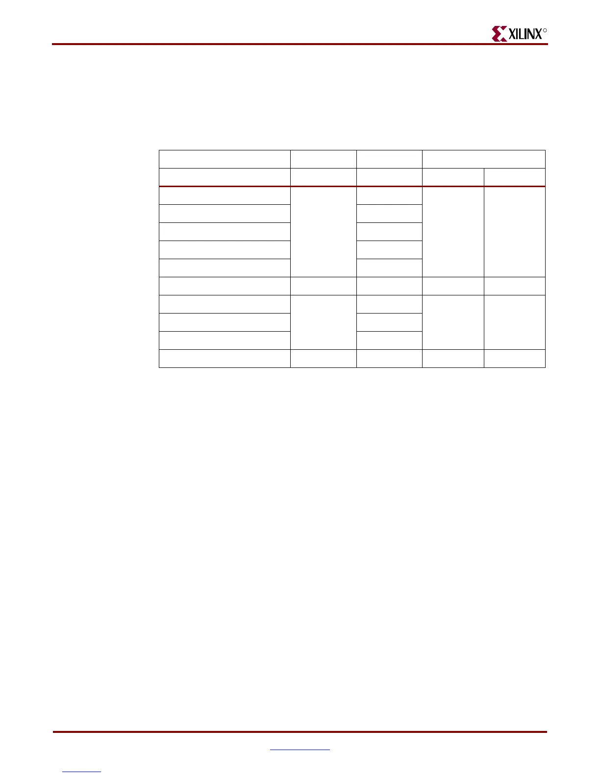
IIC Buses
The board supports four IIC buses; Main, Video, SFP, and DDR2. Each of the IIC buses has
1K pull-ups on its SCL and SDA signals. Table 1-35 describes the IIC devices attached to
each of the four buses.
Table 1-35: IIC Bus Connections
IIC FPGA Pins
Device Bus Name Address SCL SDA
EEPROM IC
Main
0x50
F9 F8
Fan Controller IC 0x2C
Clock Gen IC 0x6A
Clock Gen IC 0x6A
Expansion Hdr N/A
SFP Cage SFP N/A R26 U28
DVI Output: Codec IC
Video
0x76
U27 T29DVI Output: Connector N/A
VGA Input: Codec IC 0x4C
DDR2 DDR2 SPD 0x50 E29 F29
Downloaded from Elcodis.com electronic components distributor