ML505/ML506/ML507 Evaluation Platform www.xilinx.com 19
UG347 (v3.1.1) October 7, 2009
Detailed Description
R
DDR2 Memory Expansion
The DDR2 interface support user installation of SODIMM modules with more memory
since higher order address and chip select signals are also routed from the SODIMM to the
FPGA.
DDR2 Clock Signal
Two matched length pairs of DDR2 clock signals are broadcast from the FPGA to the
SODIMM. The FPGA design is responsible for driving both clock pairs with low skew. The
delay on the clock trace is designed to match the delay of the other DDR2 control signals.
DDR2 Signaling
All DDR2 SDRAM control signals are terminated through 47Ω resistors to a 0.9V VTT
reference voltage. The FPGA DDR2 interface supports SSTL18 signaling and all DDR2
signals are controlled impedance. The DDR2 data, mask, and strobe signals are matched
length within byte groups. The ODT functionality of the SODIMM should be utilized.
3. Differential Clock Input and Output with SMA Connectors
High-precision clock signals can be input to the FPGA using differential clock signals
brought in through 50Ω SMA connectors. This allows an external function generator or
other clock source to drive the differential clock inputs that directly feed the global clock
input pins of the FPGA. The FPGA can be configured to present a 100Ω termination
impedance.
A differential clock output from the FPGA is driven out through an LVDS clock
multiplexer (U12) onto a second pair of SMA connectors (J12 and J13). This allows the
FPGA to drive a precision clock to an external device such as a piece of test equipment.
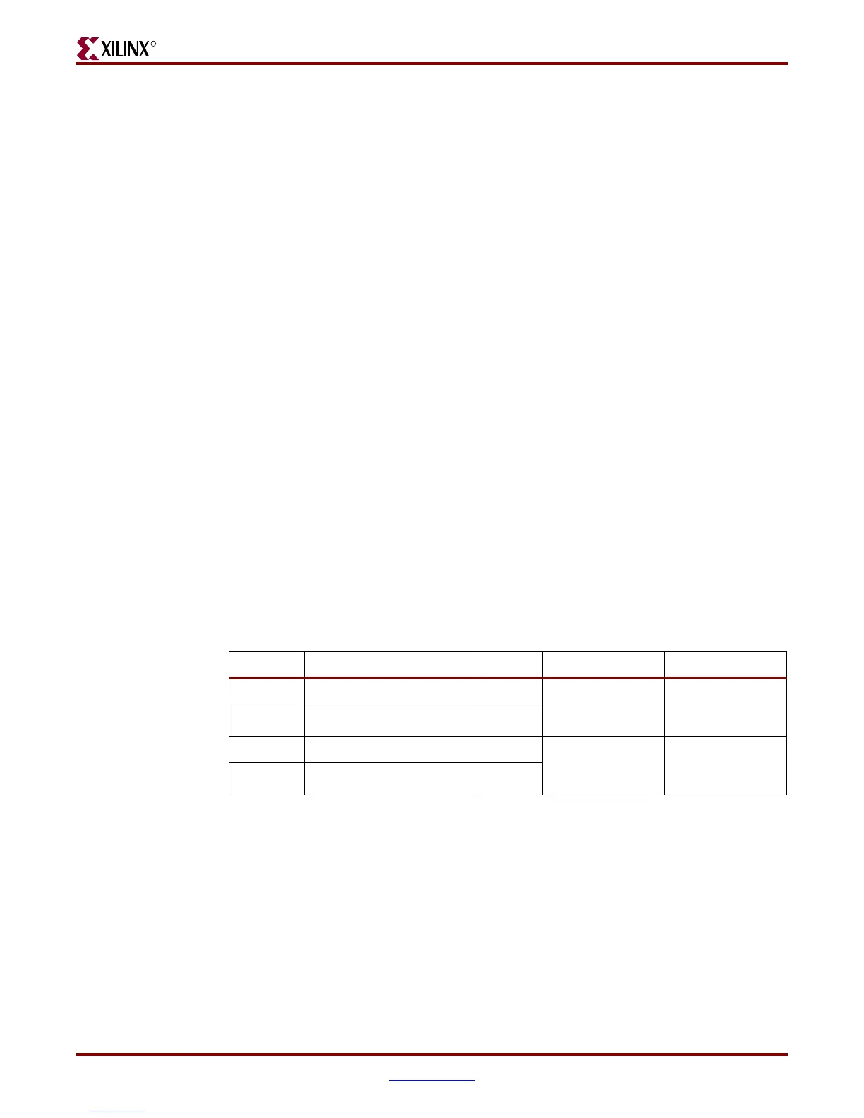
Table 1-3 summarizes the differential SMA clock pin connections.
4. Oscillators
The board has one crystal oscillator socket (X1) wired for standard LVTTL-type oscillators.
It connects to the FPGA clock pin as shown in Table 1-4, page 20. The X1 socket is
populated with a 100-MHz oscillator and is powered by the 3.3V supply.
The board also provides an IDT5V9885 (U8) EEPROM programmable clock generator
device. This device is used to generate a variety of clocks to the board peripherals and
Table 1-3: Differential SMA Clock Connections
Connector Clock Name FPGA Pin ML505/ML506 ML507
J10 SMA_DIFF_CLK_IN_P H14 GTP1 of
GTP_X0Y4
receive pair
GTX1 of
GTX_X0Y5
receive pair
J11 SMA_DIFF_CLK_IN_N H15
J12
(1)
SMA_DIFF_CLK_OUT_P J20 GTP1 of
GTP_X0Y4
transmit pair
GTX1 of
GTX_X0Y5
transmit pair
J13
(1)
SMA_DIFF_CLK_OUT_N J21
Notes:
1. When jumper J54 (located near the battery) is not shunted (default), the FPGA differential clock output
is selected on U12 and driven out to the SMA connectors, J12 and J13.
Downloaded from Elcodis.com electronic components distributor