ML505/ML506/ML507 Evaluation Platform www.xilinx.com 23
UG347 (v3.1.1) October 7, 2009
Detailed Description
R
Single-Ended Expansion I/O Connectors
Header J6 contains 32 single-ended signal connections to the FPGA I/Os. This permits the
signals on this connector to carry high-speed, single-ended data. All single-ended signals
on connector J6 are matched length traces. The V
CCIO
of these signals can be set to 2.5V or
3.3V by setting jumper J20. Table 1-10 summarizes the single-ended connections on this
expansion I/O connector.
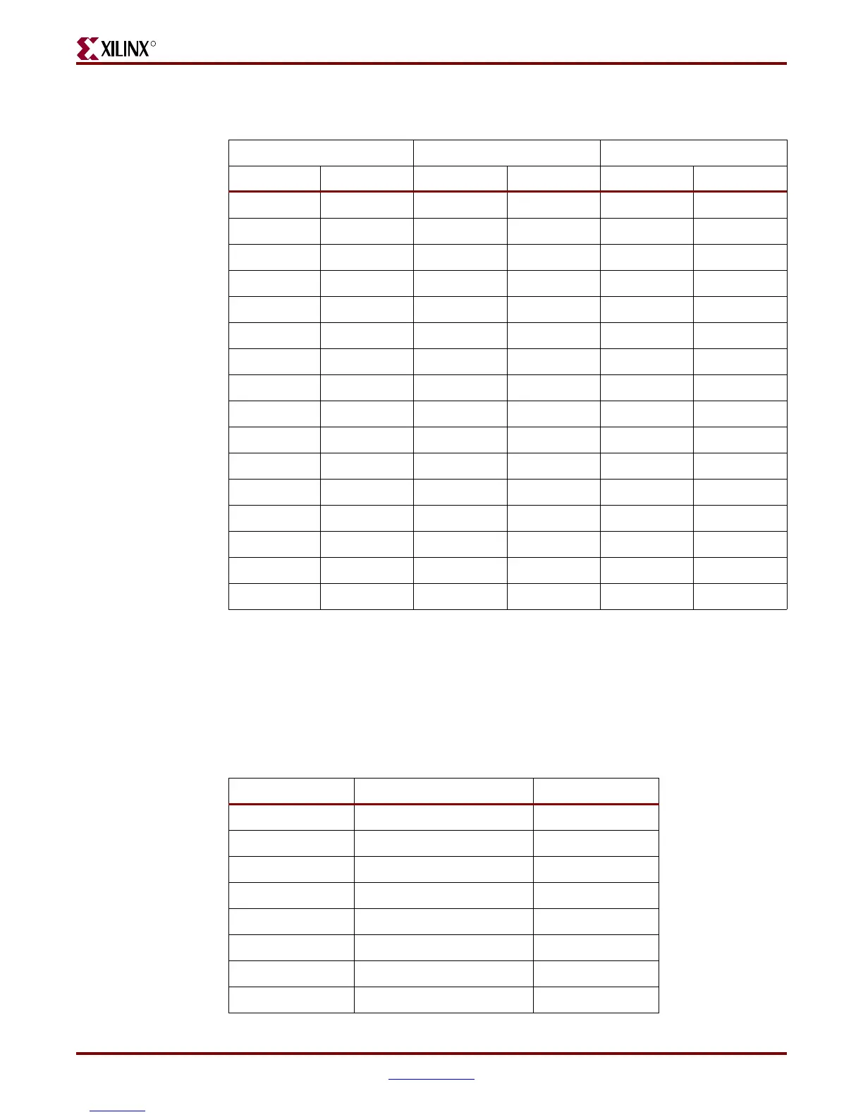
Table 1-9: Expansion I/O Differential Connections (J4)
J4 Differential Pin Pair Schematic Net Name FPGA Pin
Pos Neg Pos Neg Pos Neg
4 2 HDR2_4 HDR2_2 L34 K34
8 6 HDR2_8 HDR2_6 K33 K32
12 10 HDR2_12 HDR2_10 P32 N32
16 14 HDR2_16 HDR2_14 T33 R34
20 18 HDR2_20 HDR2_18 R33 R32
24 22 HDR2_24 HDR2_22 U33 T34
28 26 HDR2_28 HDR2_26 U32 U31
32 30 HDR2_32 HDR2_30 V32 V33
36 34 HDR2_36 HDR2_34 W34 V34
40 38 HDR2_40 HDR2_38 Y33 AA33
44 42 HDR2_44 HDR2_42 AF34 AE34
48 46 HDR2_48 HDR2_46 AF33 AE33
52 50 HDR2_52 HDR2_50 AC34 AD34
56 54 HDR2_56 HDR2_54 AC32 AB32
60 58 HDR2_60 HDR2_58 AC33 AB33
64 62 HDR2_64 HDR2_62 AN32 AP32
Table 1-10: Expansion I/O Single-Ended Connections (J6)
J6 Pin Schematic Net Name FPGA Pin
2 HDR1_2 H33
4 HDR1_4 F34
6 HDR1_6 H34
8 HDR1_8 G33
10 HDR1_10 G32
12 HDR1_12 H32
14 HDR1_14 J32
16 HDR1_16 J34
Downloaded from Elcodis.com electronic components distributor