ML505/ML506/ML507 Evaluation Platform www.xilinx.com 43
UG347 (v3.1.1) October 7, 2009
Detailed Description
R
40. PCI Express Interface
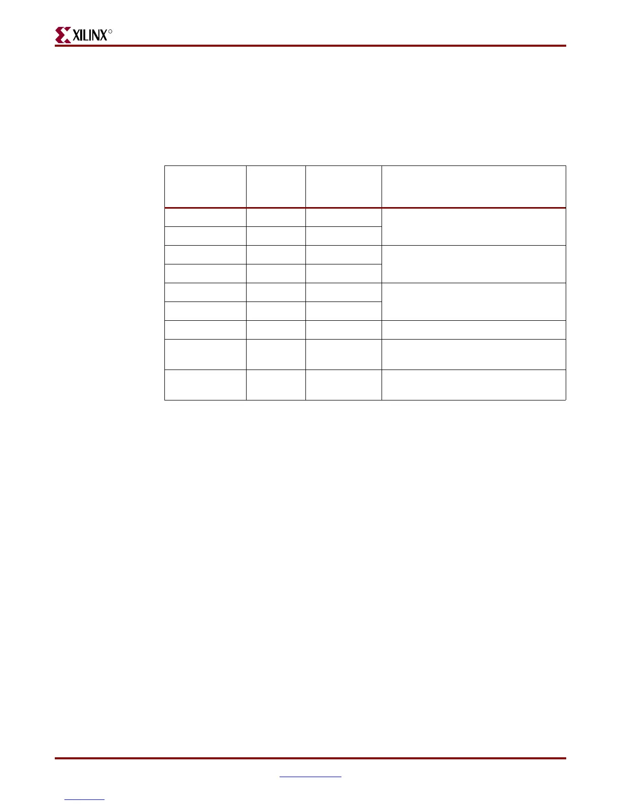
Table 1-25 shows the PCIe connector (P21) that provides single-lane access through the
RocketIO transceivers to the Virtex-5 FPGA integrated Endpoint block for PCIe designs.
See the
Virtex-5 FPGA Integrated Endpoint Block User Guide for PCI Express Designs [Ref 11] for
more information.
Table 1-25: PCIe Connection to FPGA
Pin Name
FPGA Pin
(U1)
Edge
Connector Pin
(P21)
Description
PCIE_RX_N AF1 B15
Integrated Endpoint block receive pair
PCIE_RX_P AE1 B14
PCIE_TX_N AE2 A17
Integrated Endpoint block transmit pair
PCIE_TX_P AD2 A16
PCIE_CLK_N AF3 A14
Integrated Endpoint block differential
clock pair from PCIe edge connector
PCIE_CLK_P AF4 A13
PCIE_PRSNT_B AF24 A1, B17 Integrated Endpoint block present signal
PCIE_PERST_B - A11
Integrated Endpoint block reset signal
available on CPLD
PCIE_WAKE_B - B11
Integrated Endpoint block wake signal
available on CPLD
Notes:
1. For ML505/ML506 platforms, access is through GTP0 of GTP_X0Y1.
2. For ML507 platforms, access is through GTX0 of GTX_X0Y2.
Downloaded from Elcodis.com electronic components distributor