EasyManuals Logo

Xilinx Virtex-5 FPGA ML561 User Manual

Xilinx Virtex-5 FPGA ML561
140 pages
To Next Page IconTo Next Page
To Previous Page IconTo Previous Page
Page #73 background imageLoading...
Page #73 background image
Virtex-5 FPGA ML561 User Guide www.xilinx.com 73
UG199 (v1.2.1) June 15, 2009
Signal Integrity Correlation Results
R
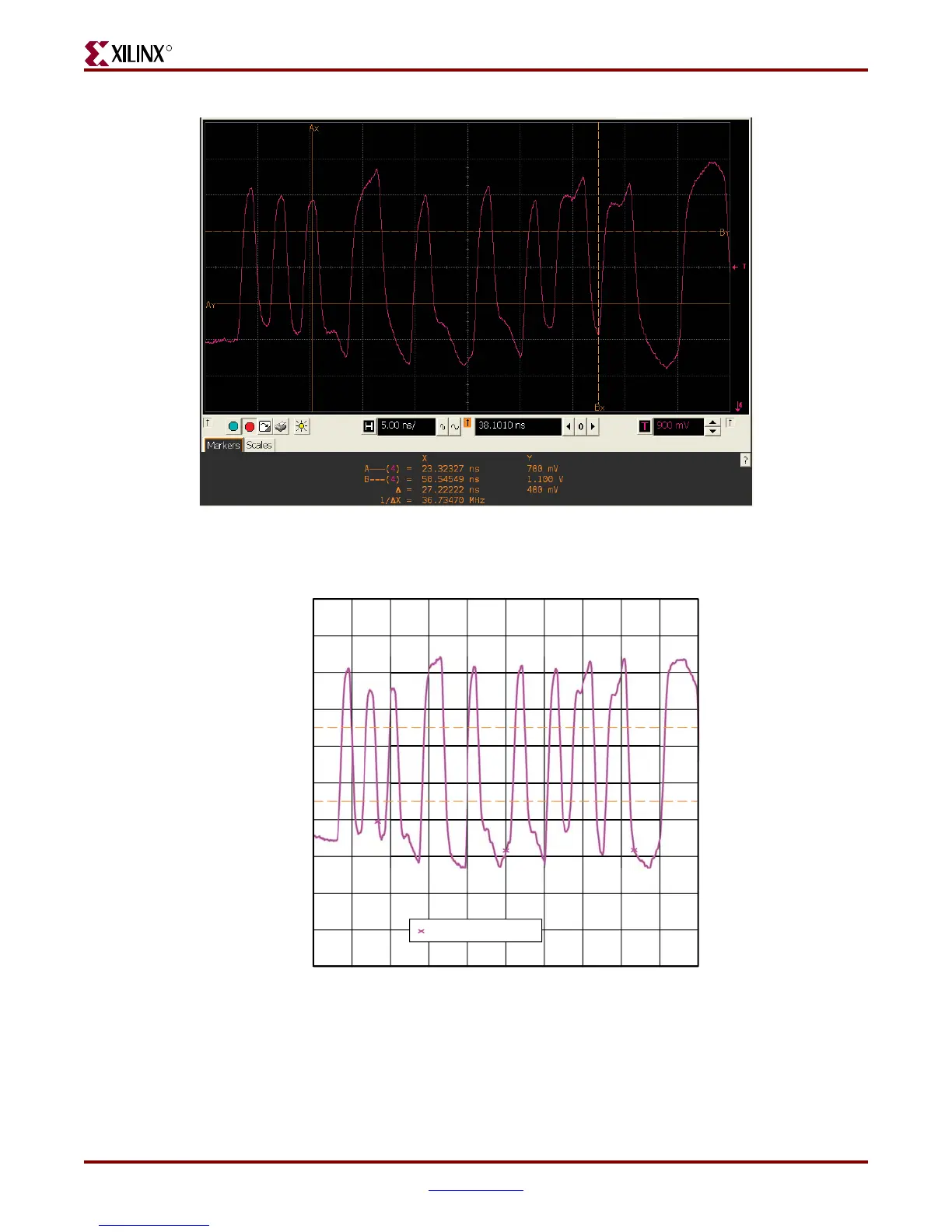
Figure 7-24: DDR2 DIMM Write HW Measurement - Waveform Scope Shot at Probe Point #1 (DDR2 Memory
Via)
UG199_c7_24_071107
Figure 7-25: DDR2 DIMM Write Correlation - Waveform Scope Shot at Probe Point #1 (Slow Corner)
95.000 105.000 115.000 125.000 135.000 145.000
-200.0
0.000
200.0
400.0
600.0
800.0
1000.0
1200.0
1400.0
1600.0
1800.0
UG199_c7_23_071007
Time (ns)
Voltage (mV)
Probe 3:C13.1 (at pin)

Table of Contents

Questions and Answers:

Question and Answer IconNeed help?

Do you have a question about the Xilinx Virtex-5 FPGA ML561 and is the answer not in the manual?

Xilinx Virtex-5 FPGA ML561 Specifications

General IconGeneral
BrandXilinx
ModelVirtex-5 FPGA ML561
CategoryMotherboard
LanguageEnglish

Related product manuals