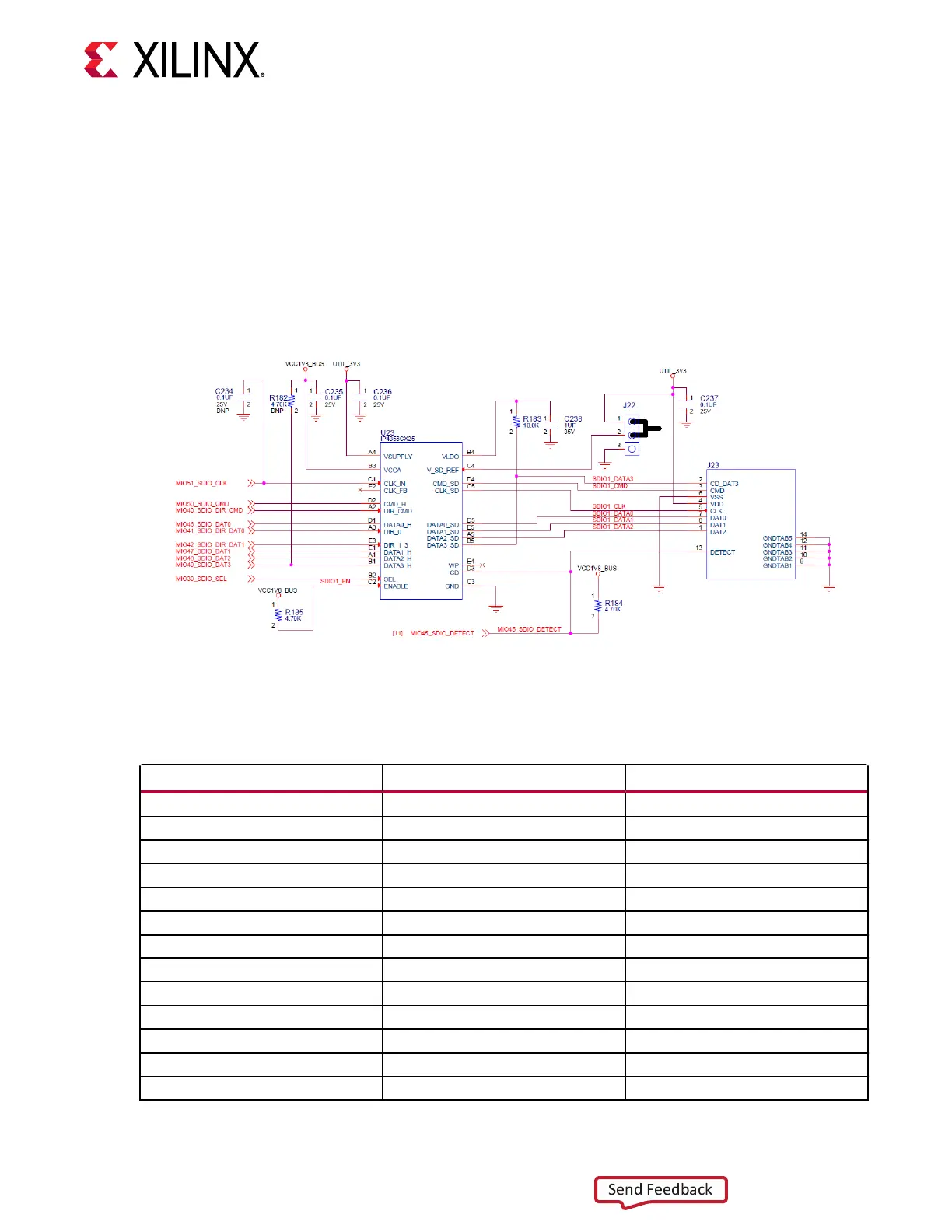
The SDIO signals are connected to ZU48DR RFSoC PS bank 501 which has its VCCMIO set to
1.8V. The SD interface nets MIO[46:49]_SDIO_DAT[0:3], MIO50_SDIO_CMD, and
MIO51_SDIO_CLK each have a series 30Ω resistor at the Bank 501 source. An NXP
IP4856CX25 SD 3.0-compliant voltage level-translator U23 is present between the ZU48DR
RFSoC and the SD card connector (J23). The NXP IP4856CX25 U23 device provides SD3.0
capability with SDR104 performance.
The following gure shows the connecons of the SD card interface on the ZCU208 board.
Figure 10: SD Card Interface
The NXP SD3.0 level shier is mounted on an Aries adapter board that has the pin mapping
shown in the following table.
Table 15: IP4856CX25 U23 Adapter Pinout
Aires Adapter Pin Number IP4856CX25 U23 Pin Number IP4856CX25 U23 Pin Name
1 C1 CLK_IN
2 C3 GND
3 D3 CD
4 D2 CMD_H
5 E2 CLK_FB
6 E4 WP
7 B4 VLDO
8 C4 VSD_REF
9 A3 DIR_0
10 A4 VSUPPLY
11 B3 VCCA
12 A2 DIR_CMD
13 D1 DATA0_H
Chapter 3: Board Component Descriptions
UG1410 (v1.0) July 8, 2020 www.xilinx.com
ZCU208 Board User Guide 37

 Loading...