A
1
2
3
4
5
6
7
8
9
10
BCDEFGH I JK
L MN
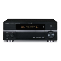
RX-V1700/DSP-AX1700
104
★ All voltages are measured with a 10MΩ/V DC electronic voltmeter.
★ Components having special characteristics are marked s and must be replaced
with parts having specifications equal to those originally installed.
★ Schematic diagram is subject to change without notice.
DSP 2/3
0
3.2
0
1.5
3.33.3
3.3
3.3
0
0.2
3.2
0.4
1.2
0.3
0
0
0.4
0.5
3.3
3.3
3.3
1.2
0
0.2
0.4
1.1
0.3
0.3
3.3
0.3
0
0
0.4
1.2
2.8
3.2
3.3
0
1.7
2.9
0
0
1.4
0
0
0
0
0
3.3
0
0
0
1.2
0
1.2
0
1.2
2.5
1.5
3.1
0
1.2
3.2
3.2
3.2
0.3
0
0
0.4
1.0
0
1.0
3.3
0
3.1
0
3.2
0
3.2
3.3
1.2
3.2
0
3.3
0
3.3
0
3.2
3.3
3.3
0
0.2 0
5.8 4.6
1.4
4.84.9
2.2
4.9
4.8
00
0
3.32.5
1.2
1.2
00
0
2.2
2.2
1.2
2.5
2.5
3.3
-0.1-0.1
4.6
3.3
4.3
5.0 5.3
0
0
0
5.3
5.1
5.8
0
2.7
2.2
2.2
4.6
0.4
0
0.4
0.3
3.3
0.3
0
0
0.4
2.8
3.3
3.2
1.7
3.3
0
0
0
2.9
2.9
0.3
0
3.3 03.2
00
0
0.2
2.8 0.2
0.4
0.4
0.3
0.3
0.3
0.2
3.3
0.3
0.4
0
0.5
0.4
3.3
2.8
3.2
0
3.2
3.2
0
0
0
3.2
3.2
0
0
2.9
2.9
0.3
3.2
0
0
0
0
0.5
0.4
3.3
0.2
0.3
0
0.4
0.2
3.3
3.3
3.3
3.3
3.3
0
3.3
2.8
0
0
0
3.2
3.3
0
2.8
3.3
0
1.2
0
0
0
3.2
1.2
0.3
2.9
0
3.3
2.9
0
0
1.2
0
0
0
3.3
0
0
0
0
0
1.2
0
3.3
0
0
0
3.2
0
1.2
3.2
3.2
0
3.2
0
0
0
0
1.2
0
0
1.2
1.2
0
3.2
3.2
3.2
0
3.3
3.2
1.2
3.2
3.2
0
0
00 0
3.2 3.2 3.1 0.3
03.2
3.2 0
3.2 4.9
3.2 4.8
3.1 4.9
3.1
4.9
2.3
4.9
2.0 3.3
2.4
3.3
0
3.2 3.2
00
3.23.2
5.1 4.9
3.3
0
4.9 4.9
4.9
4.9 4.9 4.7 -0.1
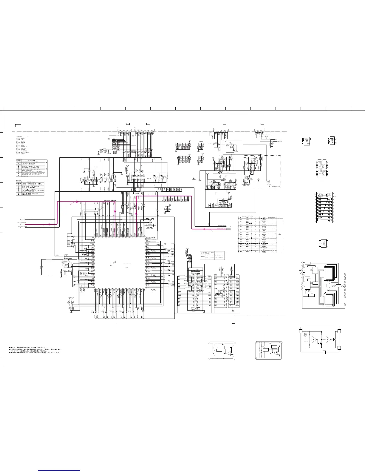
DIGITAL IN
ANALOG IN
ANALOG IN
1000/16
5
1
2
3
4
DSP
DECODER
RAM
No replacement part available.
サービス部品供給なし
U, C models
To DSP 1/3
To DSP 3/3
Y4
B2
GND 3
IC532, 533: SN74AHCT1G32DCKR
Single 2-input positive-OR gate
Vcc5A1
4B13
4A12
4Y11
3B10
3A9
3Y8
1B 2
1Y 3
2A 4
2B 5
2Y 6
GND 7
IC535: SN74AHCT08PWR
Quadruple 2-input positive-AND gates
Vcc141A 1
Y4
B2
GND 3
IC531: SN74AHC1G08DCKR
2-input positive-AND gate
Vcc5A1
IC539: W9816G6CH -7
512K x 2 banks x 16 bits SDRAM
CLOCK
BUFFER
ADDRESS
BUFFER
CLK 35
18
CKE 34
A10 20
CS
17RAS
16CAS
15WE
21A0
〜
24A3
27A4
〜
32A9
19BA
2DQ0
3DQ1
5DQ2
6DQ3
8DQ4
9DQ5
11 DQ6
12 DQ7
39 DQ8
40 DQ9
42 DQ10
43 DQ11
45 DQ12
46 DQ13
48 DQ14
49 DQ15
14 LDQM
36 UDQM
COMMAND
DECODER
REFRESH
COUNTER
REFRESH
COUNTER
DQ
BUFFER
COLUMN
COUNTER
MODE
REGISTER
CONTROL
SIGNAL
GENERATOR
CELL ARRAY
BANK #0
R
O
W
D
E
C
O
D
E
R
COLUMN DECODER
SENSE AMPLIFIER
CELL ARRAY
BANK #1
R
O
W
D
E
C
O
D
E
R
COLUMN DECODER
SENSE AMPLIFIER
1
DIR
A1
A2
A3
A4
A5
A6
A7
A8
GND
Vcc
OE
B1
B2
B3
B4
B5
B6
B7
B8
2
3
4
5
6
7
8
9
10
20
19
18
17
16
15
14
13
12
11
IC536: SN74LV245APWR
Octal bus transceiver with 3-state outputs
Y4
B2
GND 3
IC537, 538: SN74AHC1G08DCKR
2-input positive-AND gate
Vcc5A1
IC541: NJM2885DL1-25
Low dropout voltage regulator
Ther mal
Protection
Bandgap
Reference
V
OUT
V
IN
GND
13
2
IC544: NJM2885DL1-33
Low dropout voltage regulator
Ther mal
Protection
Bandgap
Reference
V
OUT
V
IN
GND
13
2
VDD
CD
RD
12
3
5
Vref
OUT
GND
IC542: R3112N421A-TR-F
Low voltage detector with output delay
to FL (5)_CB973
Page 118
J4
to FL (5)_CB959
Page 118 K4
to POWER (3)_CB17
Page 112 G6
to POWER (3)_CB16
Page 112 G6
 Loading...