App-12
IM 04L51B01-17EN
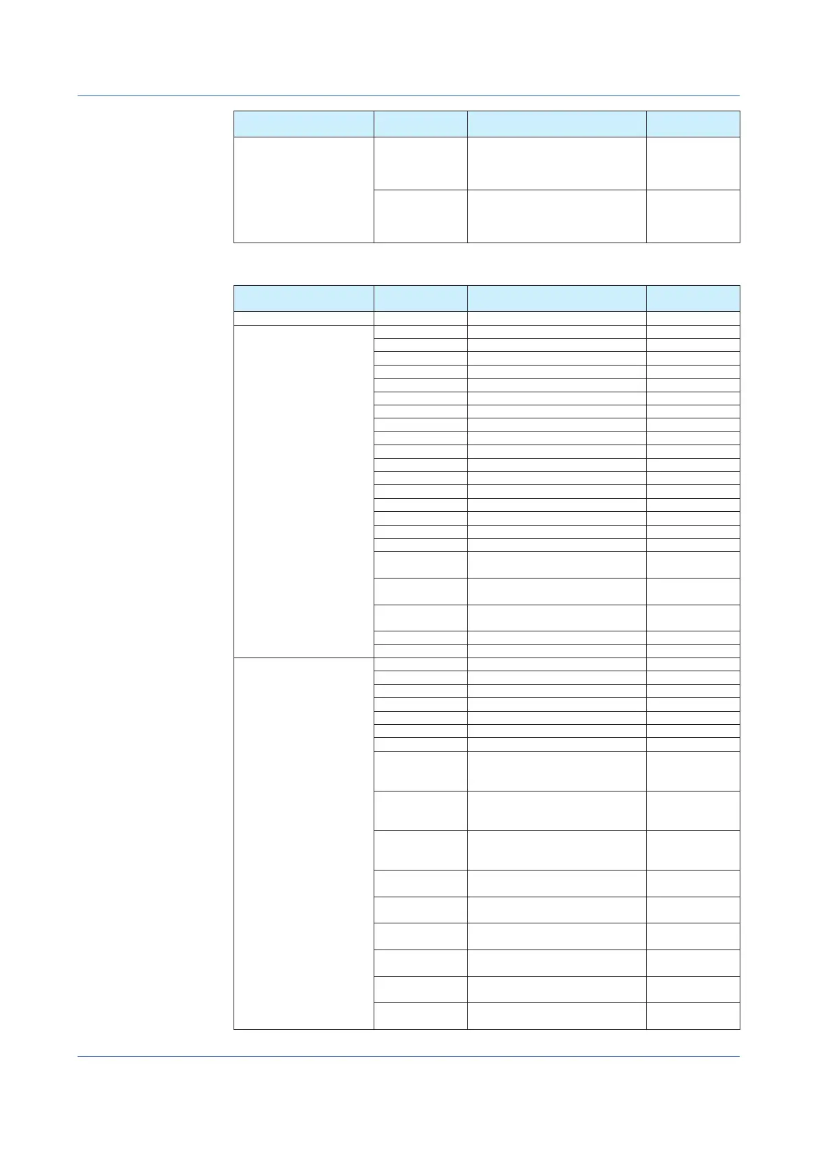
Data group name Data name Description WT Function
mark
Phase PHI_U1I2 The phase difference between the
fundamental voltage of element 1,
U1(1), and the fundamental current
of element 2, I2(1)
φ U1-I2
PHI_U1I3 The phase difference between the
fundamental voltage of element 1,
U1(1), and the fundamental current
of element 3, I3(1)
φ U1-I3
WT300
Data group name Data name Description WT Function
mark
Off - Data assignment is disabled. –
ELEMENT1 to ELEMENT3 U voltage U
I current I
P active power P
S apparent power S
Q reactive power Q
LAMBda power factor λ
PHI phase difference φ
FU voltage frequency fU
FI current frequency fI
UPPeak Maximum voltage U+pk
UMPeak Minimum voltage U-pk
IPPeak Maximum current I+pk
IMPeak Minimum current I-pk
PPPeak Maximum active power P+pk
PMPeak Minimum active power P-pk
TIME
1
Integration time Time
WH sum of watt hours WP
WHP Sum of positive P (consumed watt
hours)
WP+
WHM Sum of negative P (watt hours
returned to the power supply)
WP-
AH Sum of positive and negative
ampere hours
q
AHP Sum of positive I (ampere hours) q+
AHM Sum of negative I (ampere hours) q-
ElemHrm1 to ElemHrm3 UK_1 RMS voltage of harmonic order 1 U(1)
UK_T Rms voltage U(Total)
IK_1 RMS current of harmonic order 1 I(1)
IK_T Rms current I(Total)
PK_1 Active power of harmonic order 1 P(1)
PK_T Active power P(Total)
LAMBDA1 Power factor of harmonic order 1 λ (1)
PHIK_1 Phase difference between the
voltage and current of harmonic
order 1
φ (1)
PHIUk3 Phase difference between harmonic
voltage U(3) and the fundamental
signal U(1).
φ U(3)
PHIIk3 Phase difference between harmonic
current I(3) and the fundamental
signal I(1).
φ I(3)
UTHD Ratio of the total harmonic voltage
to U(1) or U(Total)
Uthd
ITHD Ratio of the total harmonic current
to I(1) or I(Total)
Ithd
Uhdf_1 relative harmonic content of
harmonic voltage of order 1
Uhdf(1)
Ihdf_1 relative harmonic content of
harmonic current of order 1
Ihdf(1)
Phdf_1 relative harmonic content of
harmonic power of order 1
Phdf(1)
FPLL
2
Current frequency or voltage
frequency of PLL source
fPLL
Continued on next page
Appendix 6 Data Group Name and Data Name for WT Communication

 Loading...