MC96F6432
June 22, 2018 Ver. 2.9 33
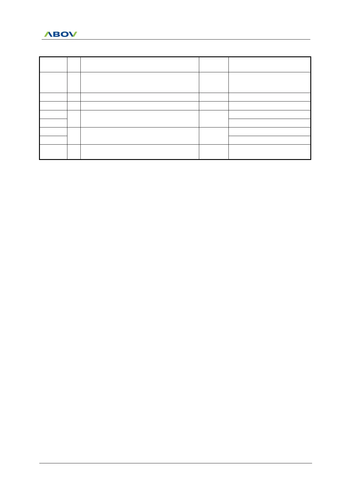
Table 5-1 Normal Pin Description (Continued)
System reset pin with a pull-up resistor when it
is selected as the RESETB by CONFIGURE
OPTION
On chip debugger data input/output
(NOTE4,5)
On chip debugger clock input
(NOTE4,5)
NOTES) 1. The P14–P17, P23–P25, P34–P37, and P43 are not in the 32-pin package.
2. The P13–P17, P22–P27, P34–P37, and P43 are not in the 28-pin package.
3. The P55/RESETB pin is configured as one of the P55 and RESETB pin by the “CONFIGURE
OPTION.”
4. If the P00/EC3/DSDA and P01/T3O/DSCL pins are connected to an emulator during the resistor
power-on reset, the pins are automatically configured as the debugger pins.
5. The P00/EC3/DSDA and P01/T3O/DSCL pins are configured as inputs with internal pull-up resistor
only during the reset or power-on reset.
6. The P50/XOUT, P51/XIN, P53/SXINT/T0O/PWM0O, and P54/SXOUT/EINT10 pins are
configured as a function pin by software control.