Amazon Store: https://www.amazon.com./alinx
Sales Email: rachel.zhou@aithtech.com
ARTIX-7 FPGA Development Board AX7035 User Manual
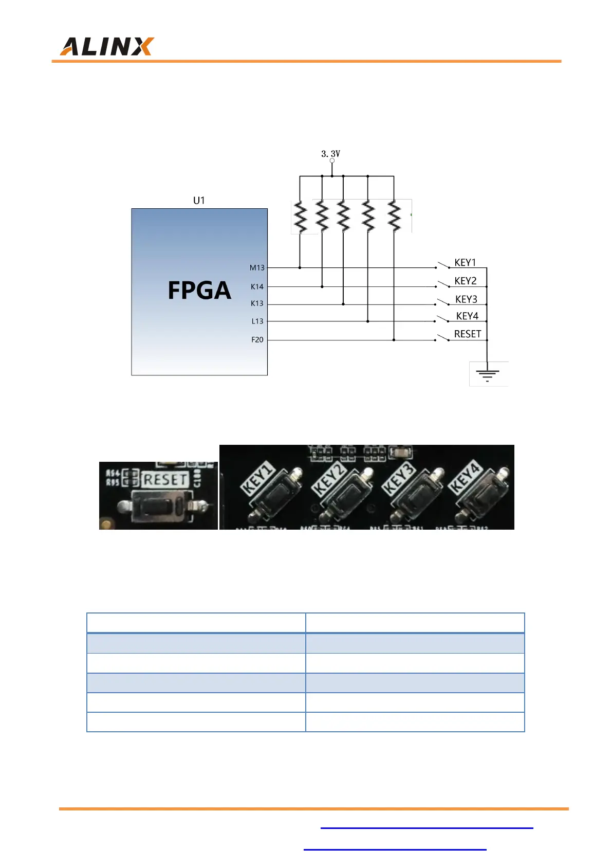
The key is active low. When the key is pressed, the IO input voltage of the
FPGA is low. When no key is pressed, The IO input voltage of the FPGA is high.
The circuit of the key part is shown in Figure 20-1.
Figure 20-1: Key Schematic
Figure 20-2: Reset Key and User Keys on the FPGA Board
Keys Pin Assignment