ZYNQ Ultrascale + FPGA Board AXU4EV-E User Manual
Amazon Store: https://www.amazon.com/alinx
Part 1: FPGA Development Board Introduction
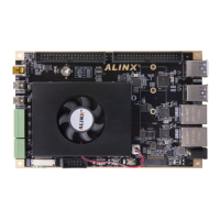
The entire structure of the AXU4EV FPGA development board is inherited
from our consistent core board + carrier board model. A high-speed inter-board
connector is used between the core board and the carrier board.
The core board is mainly composed of the smallest system of ACU4EV +
5 DDR4 + eMMC + QSPI FLASH, ACU4EV uses Xilinx's Zynq UltraScale+
MPSoCs EV chip, the model number is XCZU4EV-1SFVC784I. ZU4EV chip
can be divided into processor system part Processor System (PS) and
programmable logic part Programmable Logic (PL). On the PS side and PL
side of the ZU4EV chip, there are 4 DDR4 and 1 DDR4 respectively, each with
a capacity of up to 1GB, which enables the ARM system and FPGA system to
independently process and store data. The 8GB eMMC FLASH memory chip
and a 256Mb QSPI FLASH which are on the PS side, used to statically store
the operating system, file system and user data of MPSoCs.
The AXU4EV-E carrier board expands its rich peripheral interface,
including 1 SATA M.2 interface, 1 DP interface, 4 USB 3.0 Interface, 2 Gigabit
Ethernet interfaces, 1 SD card slot,2-Channel 40-pin expansion header,
2-Channel CAN bus interfaces, 2-Channel RS485 bus interfaces, 1 MIPI
Camera Interface and some keys and LEDs.
The following figure shows the structure of the entire development system: