Publication 1794-6.5.8 - January 2010
Communication and I/O Image Table Mapping with the DeviceNet/ControlNet Adapter 87
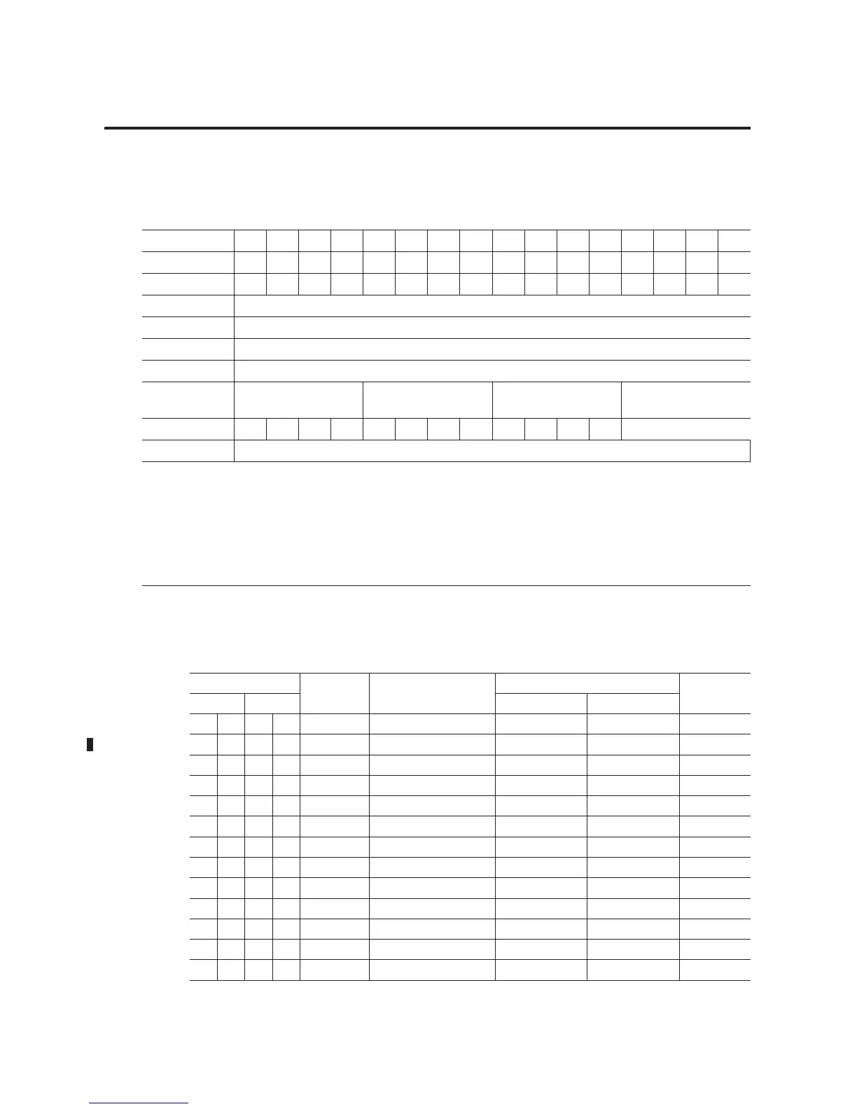
Table 5.8
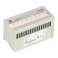
Analog Output Module (1794-OF4I) Write Configuration Block
Word/Dec. Bit 15 14 13 12 11 10 09 08 07 06 05 04 03 02 01 00
Word/Octal Bit 17 16 15 14 13 12 11 10 07 06 05 04 03 02 01 00
Write Word 1 EN S1 S0 0 0 0 0000000000
Word 2 Output Data – Channel 0
Word 3 Output Data – Channel 1
Word 4 Output Data – Channel 2
Word 5 Output Data – Channel 3
Word 6 Output Chnl 3
Configuration
Output Chnl 2
Configuration
Output Chnl 1
Configuration
Output Chnl 0
Configuration
Word 7 IC 1 TR IT Q3 Q2 Q1 Q0 RV QK CK GO Channel Number
Words 8 and 9 Not used
Where:
EN = Enable outputs; 0 = output follows S1/S0, 1 = output enabled
IC = Initiate configuration bit
TR = Transparent bit
IT = Interrupt Toggle bit
Q0–3 = Request for outputs to hold
RV = Revert to defaults bit
QK = Quick calibration
CK = Calibration clock
GO = Gain offset select
Table 5.9
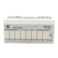
Configuring Your Outputs for the 1794-OF4I Isolated Output Module
Configuration Bits Nominal
Range
Data Type Output Values Update
Rate
MSD LSD Hexadecimal Decimal
0 0 0 1 4-20mA 2’s complement <0000–7878> <0000–30840> 5.0ms
0 0 1 0 ±10V 2’s complement <8618–79E8> <–31208–31208> 2.5ms
0 0 1 1 ±5V 2’s complement <8618–79E8> <–31208–31208> 2.5ms
0 1 0 0 0-20mA 2’s complement % 0–10000> 0–10000> 5.0ms
0 1 0 1 4-20mA 2’s complement % <0–10000> <0–10000> 5.0ms
0 1 1 0 0-10V 2’s complement % 0–10000> 0–10000> 5.0ms
0 1 1 1 ±10V 2’s complement <–10000–10000> <–10000–10000> 5.0ms
1 0 0 0 0-20mA binary 0000–F3CF> 0000–62415> 2.5ms
1 0 0 1 4-20mA binary 0000–F0F1> 0000–61681> 5.0ms
1 0 1 0 0-–10V binary 0000–F3CF> 0000–62415> 2.5ms
1 0 1 1 0-5V binary 0000–F3CF> 0000–62415> 2.5ms
1 1 0 0 ±20mA offset binary <8000–F9E8> 32768–63976> 2.5ms
1 1 0 1 4-20mA offset binary <8000–F878> <32768–63608> 5.0ms
 Loading...