Publication 1794-6.5.8 - January 2010
Communication and I/O Image Table Mapping with the DeviceNet/ControlNet Adapter 93
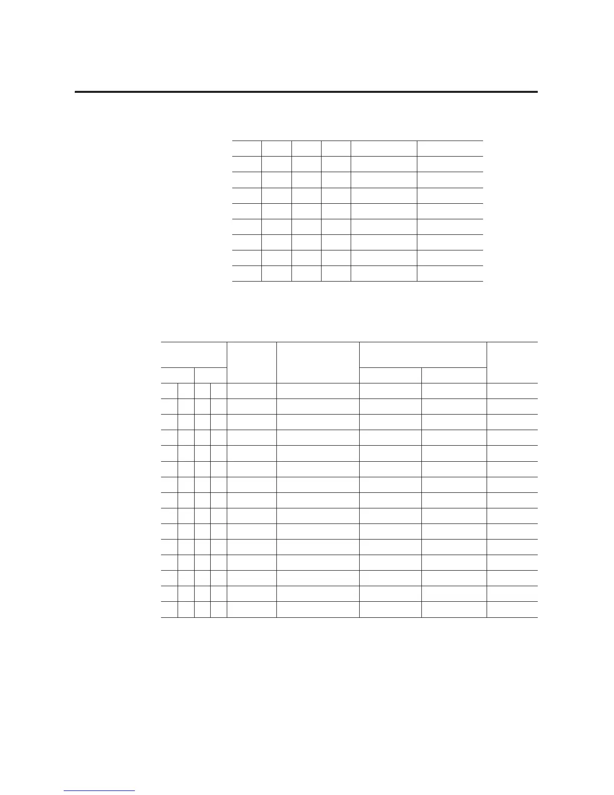
0111600Hz 1000ms low pass
1000300Hz No low pass
1001300Hz 100ms low pass
1010300Hz 500ms low pass
1011300Hz 1000ms low pass
1100150Hz No low pass
1101150Hz 100ms low pass
1110150Hz 500ms low pass
1111150Hz 1000ms low pass
Table 5.13
Setting the Input Filter
Table 5.14
Configuring Your Outputs for the 1794-IF2XOF2I Analog Combo Module
Configuration
Bits
Nominal
Range
Data Type
Output Values
(1)
Update
Rate
MSD LSD Hexadecimal Decimal
0 0 0 1 4-20mA 2’s complement <0000–7878> <0000–30840> 5.0ms
0 0 1 0 ±10V 2’s complement <8618–79E8> <–31208–31208> 2.5ms
0 0 1 1 ±5V 2’s complement <8618–79E8> <–31208–31208> 2.5ms
0 1 0 0 0-20mA 2’s complement % 0–10000> 0–10000> 5.0ms
0 1 0 1 4-20mA 2’s complement % <0–10000> <0–10000> 5.0ms
0 1 1 0 0-10V 2’s complement % 0–10000> 0–10000> 5.0ms
0 1 1 1 ±10V 2’s complement
<–10000-10000>
<–10000–10000> 5.0ms
1 0 0 0 0-20mA binary 0000–F3CF> 0000–62415> 2.5ms
1 0 0 1 4-20mA binary 0000–F0F1> 0000–61681> 5.0ms
1 0 1 0 0–10V binary 0000–F3CF> 0000–62415> 2.5ms
1 0 1 1 0-5V binary 0000–F3CF> 0000–62415> 2.5ms
1 1 0 0 ±20mA offset binary 8000–F9E8> 32768–63976> 2.5ms
1 1 0 1 4-20mA offset binary <8000–F878> <32768–63608> 5.0ms
1 1 1 0 ±10V offset binary <0618–F9E8> <1560–63976> 2.5ms
1 1 1 1 ±5V offset binary <0618–F9E8> <1560–63976> 2.5ms
(1)
< and > indicate the overrun beyond actual range (about 5%).
 Loading...