VCU118 Board User Guide 69
UG1224 (v1.5) March 15, 2023
Chapter3: Board Component Descriptions
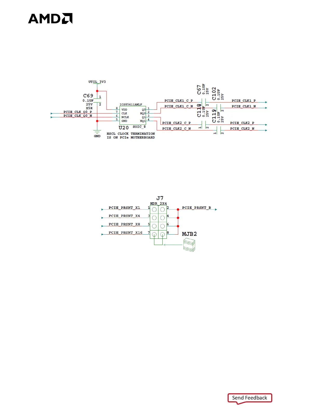
The PCIe clock is routed to a 1-to-2 ICS85411A clock buffer U20. The Q0 output of U20 is
wired to the GTY225 MGTHREFCLK0 input (see Table 3-15). The Q1 output of U20 is wired to
the GTY227 MGTHREFCLK0 input (see Table 3-17). The 1-to-2 U20 PCIe clock buffer circuit
is shown in Figure 3-11.
PCIe lane width/size is selected by jumper J7 shown in Figure 3-12. The default lane size
selection is 16-lane (J7 pins 7 and 8 jumpered).
X-Ref Target - Figure 3-11
Figure3‐11: PCIe Clock
X-Ref Target - Figure 3-12
Figure3‐12: PCI Express Lane Size Select Jumper J7