0.6 (2019–07–25)
Amlogic Proprietary and Confidential
Copyright © Amlogic. All rights reserved.
35
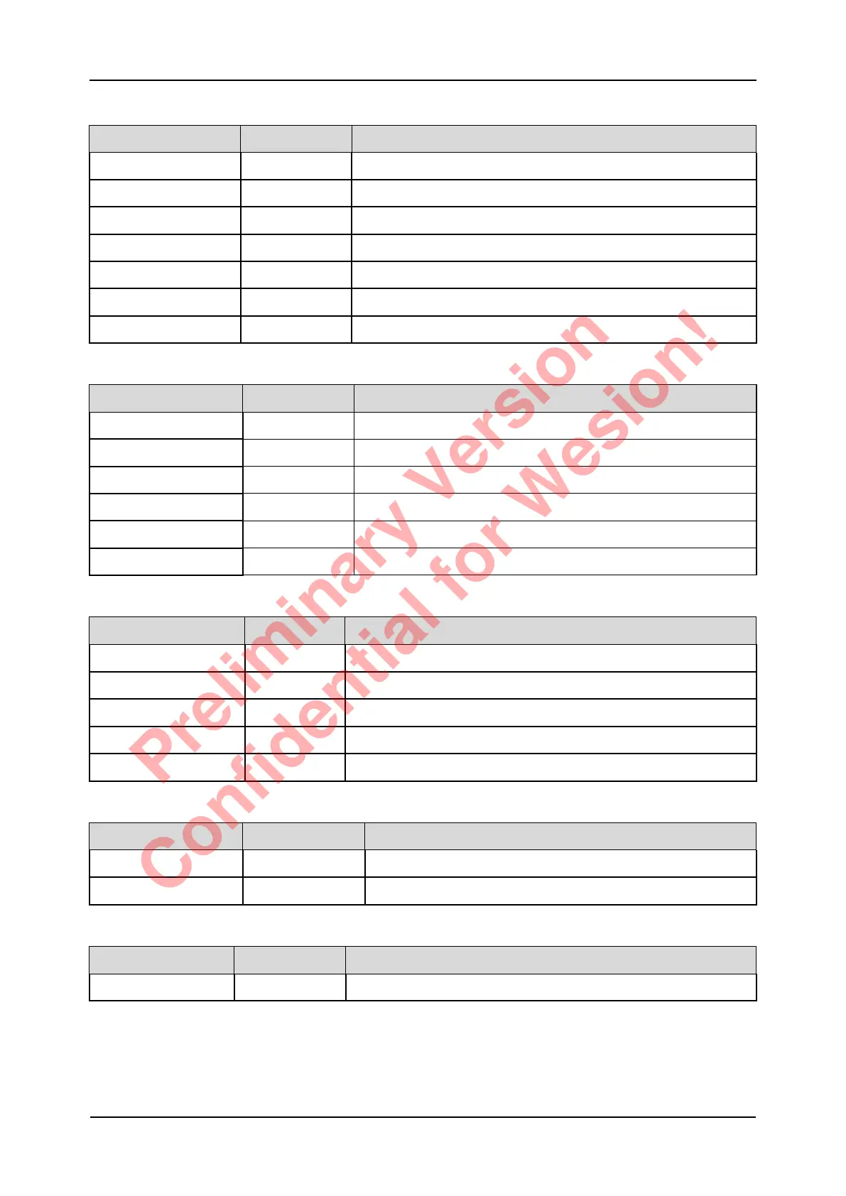
Table 4-20 NAND Signal Description
Signal Name Type Description
NAND_RB0 DI NAND ready/busy
NAND_ALE DO NAND address latch enable
NAND_CE0 DO NAND chip enable 0
NAND_CE1 DO NAND chip enable 1
NAND_CLE DO NAND command latch enable
NAND_REN_WR DO NAND read enable or write/read
NAND_WEN_CLK DO NAND write enable or clock
Table 4-21 NOR Interface Signal Description
Signal Name Type Description
NOR_CS DO SPI NOR chip select
NOR_C DO SPI NOR Serial Clock
NOR_D DIO SPI NOR 1bit mode Output, 2/4 bit mode data I/O 0
NOR_Q DIO SPI NOR 1bit mode Input, 2/4 bit mode data I/O 1
NOR_WP DIO SPI NOR Write protection output, 4 bit mode data I/O 2
NOR_HOLD DIO SPI bus hold output, 4 bit mode data I/O 3
Table 4-22 HDMI Interface Signal Description
Signal Name Type Description
HDMITX_SDA DIO HDMI TX DDC_I2C interface data signal
HDMITX_SCL DO HDMI TX DDC_I2C interface clock signal
HDMITX_HPD_IN DI HDMI TX hot-plug in signal input
AO_CEC_A DIO Customer Electronics Control signal in AO domain
AO_CEC_B DIO 2nd pin of Customer Electronics Control signal in AO domain
Table 4-23 SPDIF Interface Signal Description
Signal Name Type Description
SPDIF_IN DI SPDIF input signal
SPDIF_OUT DO SPDIF output signal
Table 4-24 PCIE Interface Signal Description
Signal Name Type Description
PCIECK_REQN DI PCIE clock request input
S905D3 Quick Reference Manual 4 Pinout Specification
Preliminary Version
Confidential for Wesion!