3.13 VGA
The following table shows the memory map for controlling a screen using the VGA interface:
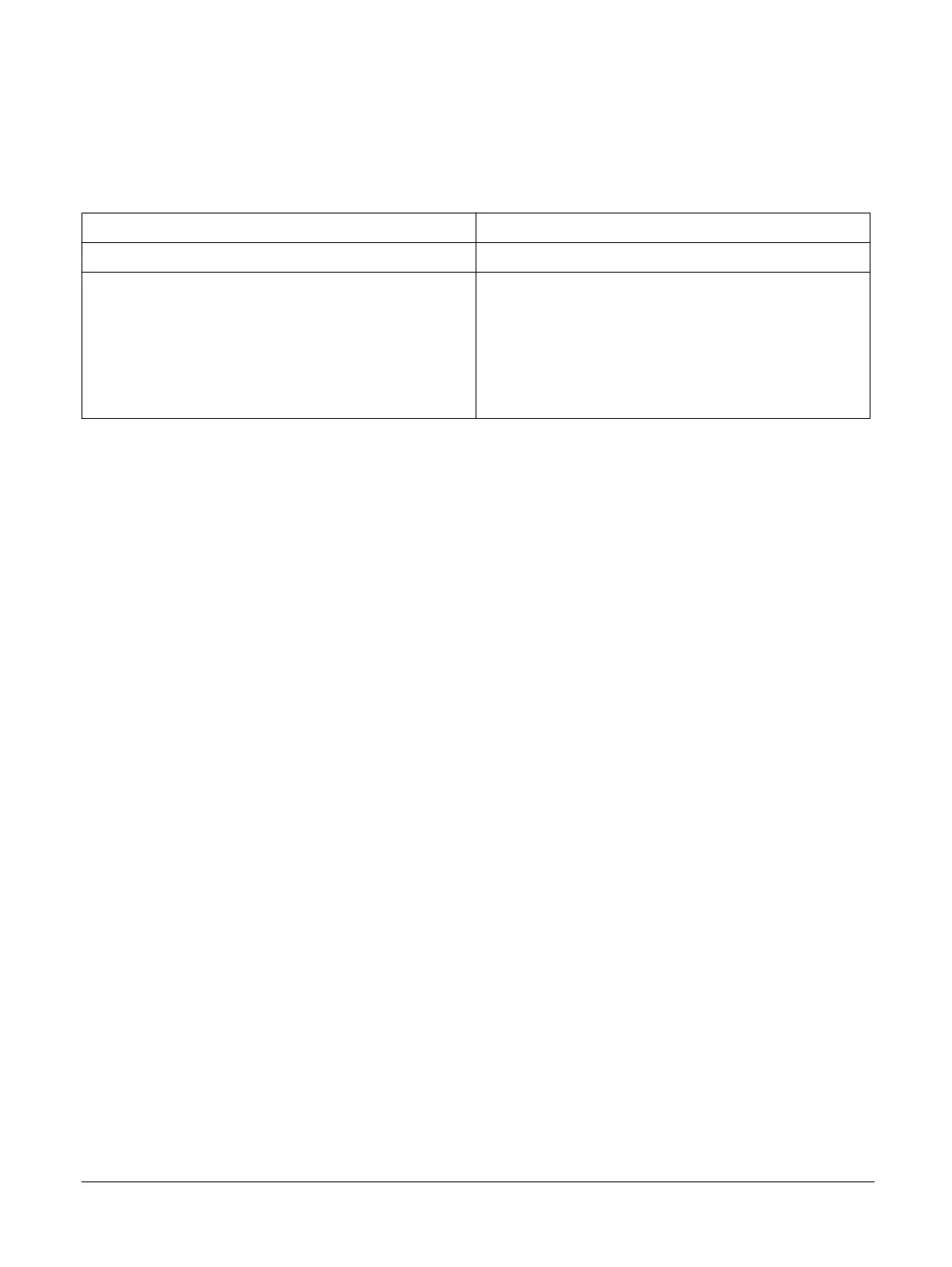
Table 3-1 VGA memory map
Address Description
0x41000000 - 0x4100FFFF Writes to the current location of the cursor.
0x41100000 - 0x4110FFFF 512x128 image area at the top right of the screen.
0x41100000 is the top left of the image area and 0x4110FFFF is
the bottom right.
Pixels are mapped into memory from the base address using an
offset address of {YYYYYYYXXXXXXXX,0b00}, where X
and Y are the horizontal and vertical pixel offset respectively.
For the image data, each pixel requires one 32-bit word, therefore, a total of 256KB are needed. The
values in the data buffer are packed as 4 bits per channel in the format 0x00000RGB.
The pixel in the top left corner of the display occupies address 0x41100000 with each successive row
using an offset of 0x00000400 from the previous row. For example: the Left-Most Pixel (LMP) of the
second row is at 0x41100400 and the LMP of the third row is at 0x41100800.
3 FPGA platform overview
3.13 VGA
ARM 100896_0000_00_en Copyright © 2017 ARM Limited or its affiliates. All rights reserved. 3-37
Non-Confidential