4.1 Source clocks
There are several source clocks for the FPGA design.
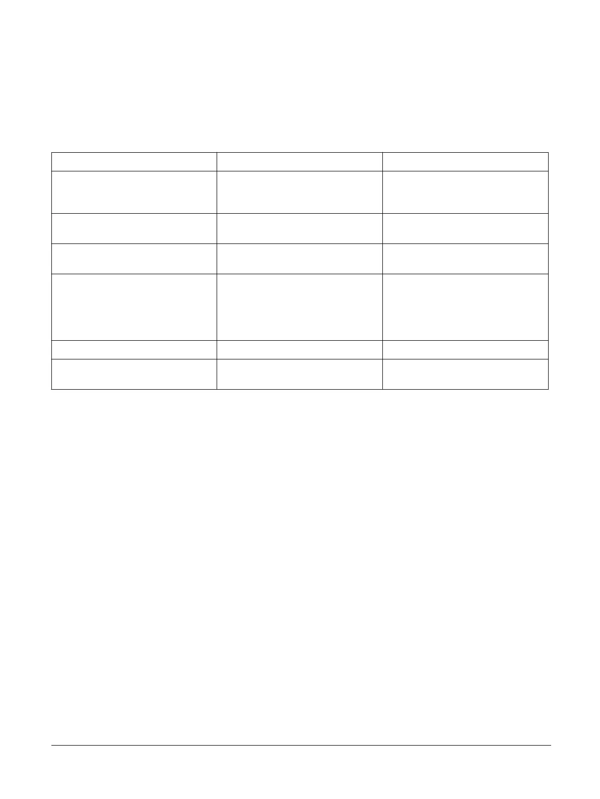
The following table shows the source clocks and their respective frequency for the system:
Table 4-1 Source clocks
Name Purpose Frequency
OSCCLK[0] Source clock for system PLL. This
generates the system processor clock and
ZBT phase shifted clock.
50MHz
OSCCLK[1] Source clock for audio PLL. This generates
two audio clocks.
24.576MHz
OSCCLK[2] Source clock to the peripherals PLL. The
output from this PLL is unused.
25MHz
CFGCLK Used by the Motherboard Configuration
Controller (MCC) to load the Serial
Communication Controller (SCC). For
more information, see the 5.1 SCC
interface overview on page 5-46.
0.5MHz
CS_TCK Debugger clock Determined by the debugger.
SPICFGCLK Used by MCC to load the software to the
ZBT memories.
7.5MHz
4 Clocks
4.1 Source clocks
ARM 100896_0000_00_en Copyright © 2017 ARM Limited or its affiliates. All rights reserved. 4-43
Non-Confidential