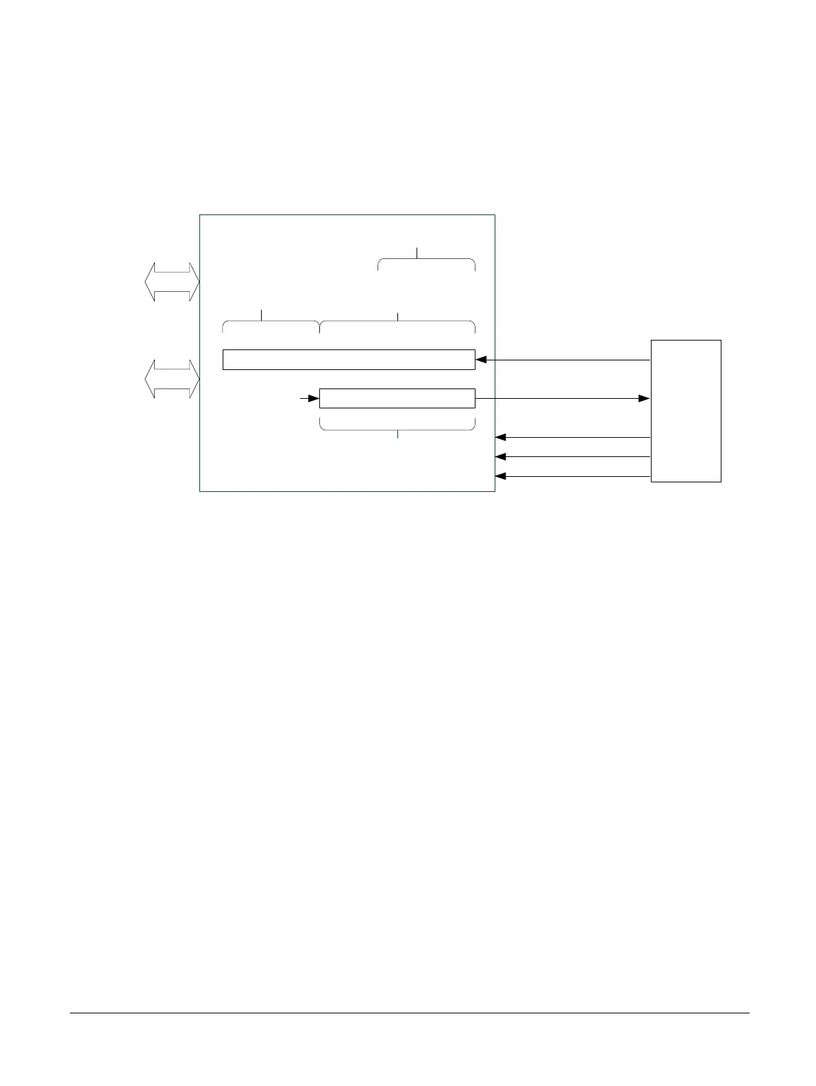
5.1 SCC interface overview
The FPGA design implements communication between the microcontroller and the FPGA system
through an SCC interface.
The following diagram provides an overview of the SCC interface:
FPGA
MCU
CFGDATAIN
CFGLOAD
CFGDATAOUT
CFGWnR
CFGCLK
0
31 0
43
Write address
3132
Write data
11
read address
0
0
Read data
fpga_scc_if.v
Read interface
Write interface
Figure 5-1 SCC interface
The read addresses and write addresses of the SCC interface do not use bits [1:0].
All address words are word-aligned.
5 Serial Communication Controller
5.1 SCC interface overview
ARM 100896_0000_00_en Copyright © 2017 ARM Limited or its affiliates. All rights reserved. 5-46
Non-Confidential