5.2 SCC memory map
The following table shows the SCC register memory map:
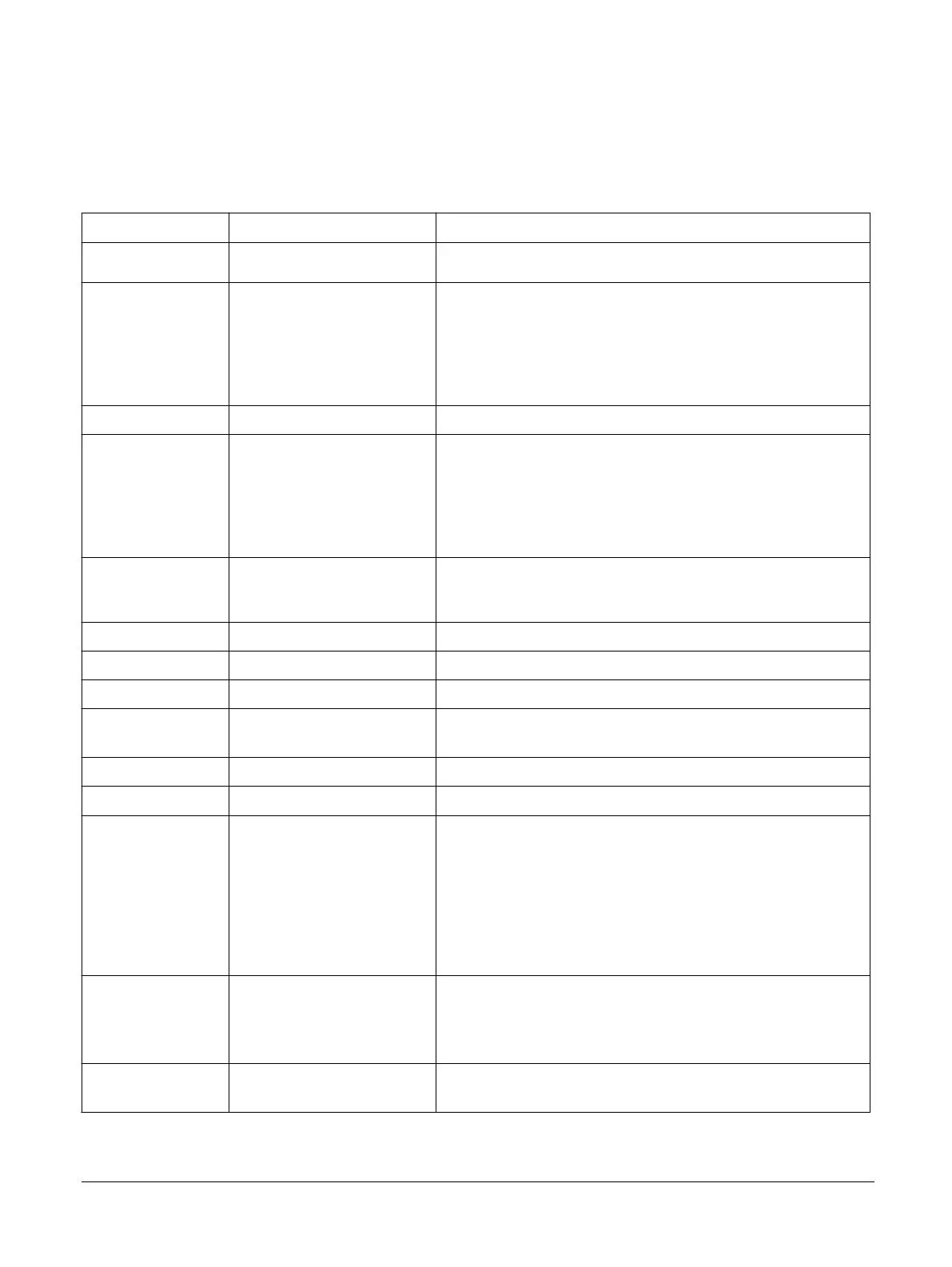
Table 5-1 SCC register memory map
Address Name Description
0x00000000
CFG_REG0
[31:0] Reserved
0x00000004
CFG_REG1
[31:8] Reserved
[7:0] Motherboard Configuration Controller (MCC) LEDs
0 Off
1 On
0x00000008
CFG_REG2 Reserved
0x0000000C
CFG_REG3
[31:8] Reserved
[7:0] MCC LEDs
0 Off
1 On
0x00000010
CFG_REG4
[31:4] Reserved
[3:0] Board revision
0x00000014
CFG_REG5 Reserved
0x00000018
CFG_REG6 Reserved
0x0000001C
CFG_REG7 Reserved
0x00000020 -
0x0000009C
- Reserved
0x000000A0
SYS_CFGDATA_RTN 32-bit serial configuration data. This is a read/write register.
0x000000A4
SYS_CFGDATA_OUT 32-bit APB configuration data. This is a read/write register.
0x000000A8
SYS_CFGCTRL
[31] Start (generates interrupt on write to this bit)
[30] Read/write access
[29:26] Reserved
[25:20] Function value
[19:12] Reserved
[11:0] Device (value of 0/1/2 for supported clocks)
0x000000AC
SYS_CFGSTAT
[31:2] Reserved
[1] Error
[0] Complete
0x000000AD –
0x000000FC
- Reserved
5 Serial Communication Controller
5.2 SCC memory map
ARM 100896_0000_00_en Copyright © 2017 ARM Limited or its affiliates. All rights reserved. 5-47
Non-Confidential