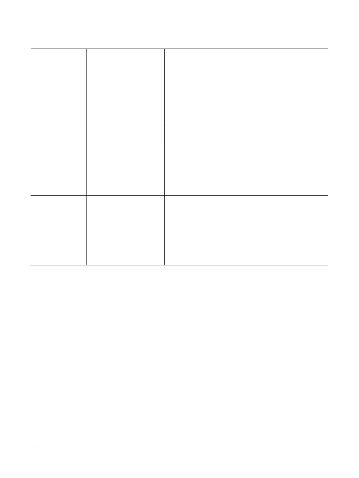
Table 5-1 SCC register memory map (continued)
Address Name Description
0x00000100
SCC_DLL DLL lock register
[31: 24] Indicate that the DLL lock is masked. These bits are mapped
to DLL LOCK MASK[7:0].
[23:16] Indicate whether the DLLs are locked or unlocked. These bits
are mapped to DLL LOCK MASK[7:0].
[15:1] Reserved
[0] Indicates whether all enabled DLLs are locked.
0x00000104 –
0x00000FF4
- Reserved
0x00000FF8
SCC_AID SCC AID register is a read-only register.
[31: 24] FPGA build number.
[23:20] V2M-MPS2+ target board revision (A = 0, B = 1).
[19:8] Reserved
[7:0] Number of SCC configuration registers.
0x00000FFC
SCC_ID SCC ID register is a read-only register.
[31: 24] Implementer ID: 0x41 = ARM
[23:20] Application note IP variant number
[19:16] IP Architecture: 0x4 =AHB
[15:12] Reserved
[11:4] Primary part number: 511 = AN511
[3:0] Reserved
5 Serial Communication Controller
5.2 SCC memory map
ARM 100896_0000_00_en Copyright © 2017 ARM Limited or its affiliates. All rights reserved. 5-48
Non-Confidential