3.16 FPGA system control and I/O
The FPGA design implements an FPGA system control block.
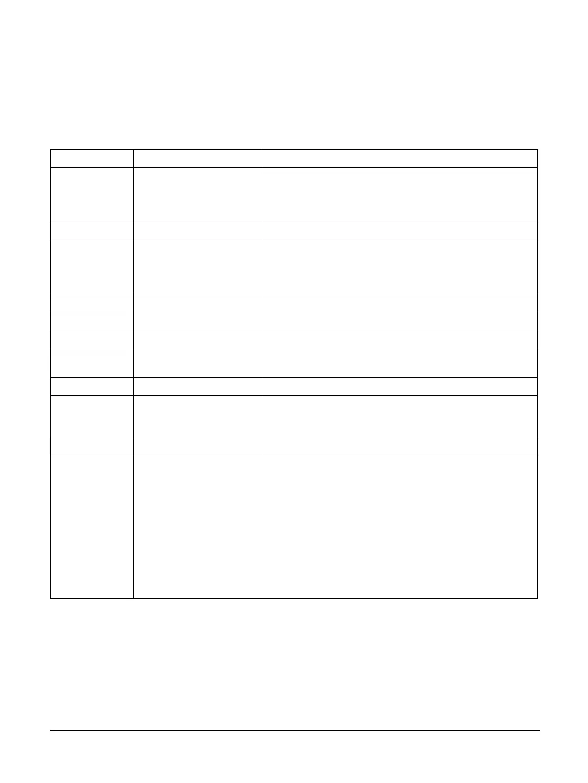
The following table shows the system control and I/O memory map:
Table 3-4 System control and I/O memory map
Address Name Description
0x40028000
LED0 LED connections
[31:2] Reserved
[1:0] LED
0x40028004
- Reserved
0x40028008
BUTTON Buttons
[31:2] Reserved
[1:0] Buttons
0x4002800C
- Reserved
0x40028010
CLK1HZ 1Hz up counter
0x40028014
CLK100HZ 100Hz up counter
0x40028018
COUNTER Cycle Up Counter Increments when the 32-bit prescale counter reaches
zero.
0x4002801C
PRESCALE Contains the reload value for the prescale counter.
0x40028020
PSCNTR 32-bit prescale counter – current value of the prescaler counter. The Cycle
Up Counter increments when the prescale down counter reaches zero. The
prescaler counter is reloaded with PRESCALE after reaching zero.
0x40028024
- Reserved
0x4002804C
MISC Miscellaneous control
[31:7] Reserved
[6] CLCD_BL_CTRL
[5] CLCD_RD
[4] CLCD_RS
[3] CLCD_RESET
[2] Reserved
[1] SPI_nSS
[0] CLCD_CS
3 FPGA platform overview
3.16 FPGA system control and I/O
ARM 100896_0000_00_en Copyright © 2017 ARM Limited or its affiliates. All rights reserved. 3-41
Non-Confidential