31
7679H–CAN–08/08
AT90CAN32/64/128
Note: 1. SRWn1 = SRW11 (upper sector) or SRW01 (lower sector), SRWn0 = SRW10 (upper sector) or
SRW00 (lower sector).
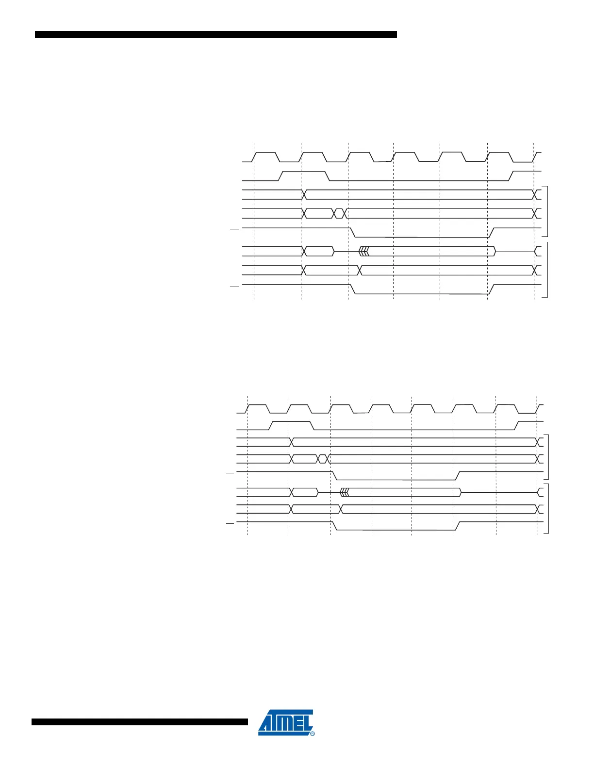
The ALE pulse in period T5 is only present if the next instruction accesses the RAM (internal
or external).
Figure 4-8. External Data Memory Cycles with SRWn1 = 1 and SRWn0 = 0
(1)
Note: 1. SRWn1 = SRW11 (upper sector) or SRW01 (lower sector), SRWn0 = SRW10 (upper sector) or
SRW00 (lower sector).
The ALE pulse in period T6 is only present if the next instruction accesses the RAM (internal
or external).
Figure 4-9. External Data Memory Cycles with SRWn1 = 1 and SRWn0 = 1
(1)
Note: 1. SRWn1 = SRW11 (upper sector) or SRW01 (lower sector), SRWn0 = SRW10 (upper sector) or
SRW00 (lower sector).
The ALE pulse in period T7 is only present if the next instruction accesses the RAM (internal
or external).
ALE
T1 T2 T3
Write
Read
WR
T6
A15:8
AddressPrev. addr.
DA7:0
Address DataPrev. data XX
RD
DA7:0 (XMBK = 0)
DataPrev. data Address
DataPrev. data Address
DA7:0 (XMBK = 1)
System Clock (CLK
CPU
)
T4 T5
ALE
T1 T2 T3
Write
Read
WR
T7
A15:8
AddressPrev. addr.
DA7:0
Address DataPrev. data XX
RD
DA7:0 (XMBK = 0)
DataPrev. data Address
DataPrev. data Address
DA7:0 (XMBK = 1)
System Clock (CLK
CPU
)
T4 T5 T6

 Loading...


