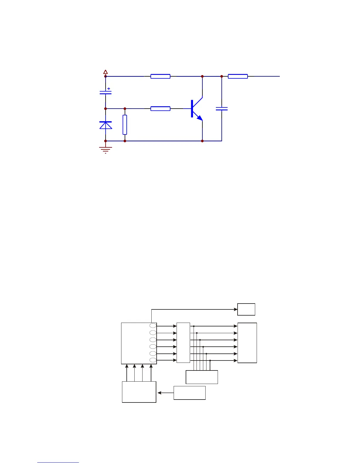
Figure 3.2.9.1 Reset circuit diagram
2. Working principle: after power on, voltage of DV33 increases to 3.3V, main chip power supply is
normal, because voltage of DV33 cannot change suddenly, Q201 base electrode has current in, Q201 is
saturated on, URST is low level; DV33 charges TC208 through R219 and Q201 emitter electrode to
make TC208 cathode voltage decrease slowly. When this voltage reduces below 0.7V, Q201 cuts off,
URST changes into high level, and the process for URST from low to high is called low level effective
reset signals by us. After power off, DV33 voltage reduces, TC208 and DV33 voltage reduce together,
D201 performs surge discharge and clamping to Tc208.
3.2.10 Audio circuit
1. Audio circuit block diagram is shown in the figure 3.2.10.1:
D201
1N4148
R219
10K
R222
33R
URST#
DV33
C272
104
R221
10K
R220
1K
TC208
47uF/10V
Q201
2SC1815-YS
GND
3.2.9 Reset circuit
1. Reset circuit is shown in the figure 3.2.9.1:
MT1389
228
227
226
224
223
222
CTR
ALS
AL
AR
ARS
SW
Audio amplifying
filtering
Mute circuit
L
R
LS
RS
C
SW
Audio
terminal
ASPDIF
IEC958
CS5340
MIC board
OK
SACLK
SBCLK
SLRCK
AMDATA
Figure 3.2.10.1 Audio circuit block diagram
AV
board
- 26 -