2. Working principle: besides from normal AV output, this player also has HDMI output. Normal AV
output is the same with that of other normal DVD players: process the analog audio and video signals
decode by, and then send to analog output terminal; digital audio output signal ASPDIF is directly send
to digital output terminal. Analog video signal and digital video signal sent by 1389 are sent to MT1392E
(U701) for processing, and digital audio signal is sent to MT1392E; MT1392E is a format conversion
processor, which switches normal audio and video signals into HDMI standard format, HDMI switches 8-
bit data into 10-bit signal through decoding and outputs in the means of differential transmission. Audio
and video signals transmit through 3 TMDS data channels. Signals outputted from MT1392E are directly
sent to HDMI jack to fulfill HDMI output. The working principle of HDMI jack is to transmit digital high
definition signals without any damage with advantages that no extra loss in the course of transmission,
digital signal and analog signal can be transmitted at the same time, transmission speed may be
increased, resolution is not controlled by SXGA, usage is simple ans cost is reduced. Digital video
signal Y0-Y7 outputs from pin 157-165 of 1389 to send to pin 13-20 of 1392E. 8-channel digital audio
signals output from pin 197, 202, 203, 209-212 of 1389 to send to pin 73-79 of 1392E, and YNC digital
audio ASPDIF of 1389 outputs from pin 216 to send to pin 72 of 1392E. Pin 182, 185, 183 of 1389 output
analog video signal R, G, B which are sent to pin 68, 70, 71 of 1392E. Clock signal 1392 VCK of 1392E
is produced by 1389 and outputs from pin 166, the communication format between 1389 and 1392E is
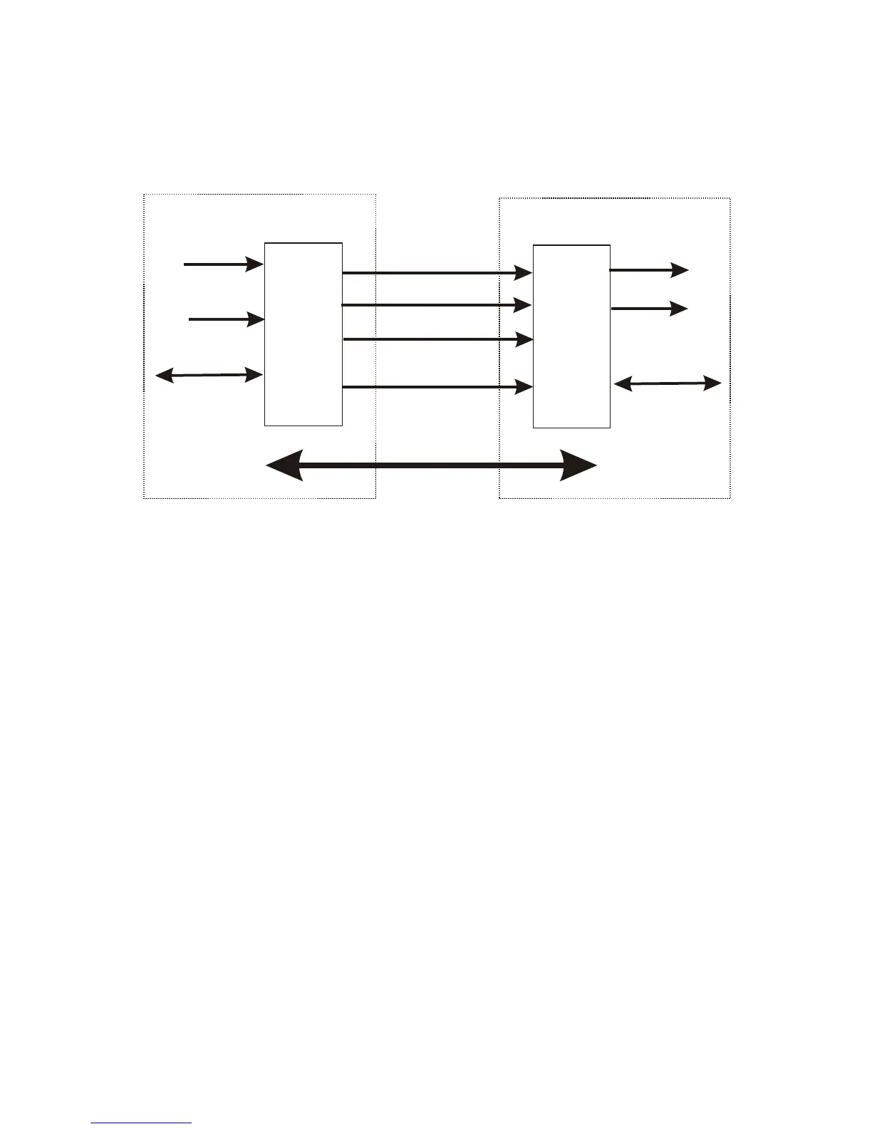
Video
HOUSE Source
HDMI Sink
Audio
Control Status
Video
Audio
Control Status
HDMI Trasmitter
HDMI Receiver
Display Data Channel
TMDS Chnanel 0
TMDS Chnanel 1
TMDS Chnanel 2
TMDS Clock Chnanel
3.2.16 HDMI circuit
1. HDMI circuit block diagram is shown in the figure 3.2.16.1, “Source” refers to device with HDMI
output jack and “Sink” refers to device with HDMI input.
Figure 6 HDMI circuit block diagram3.2.1 .1
- 32 -