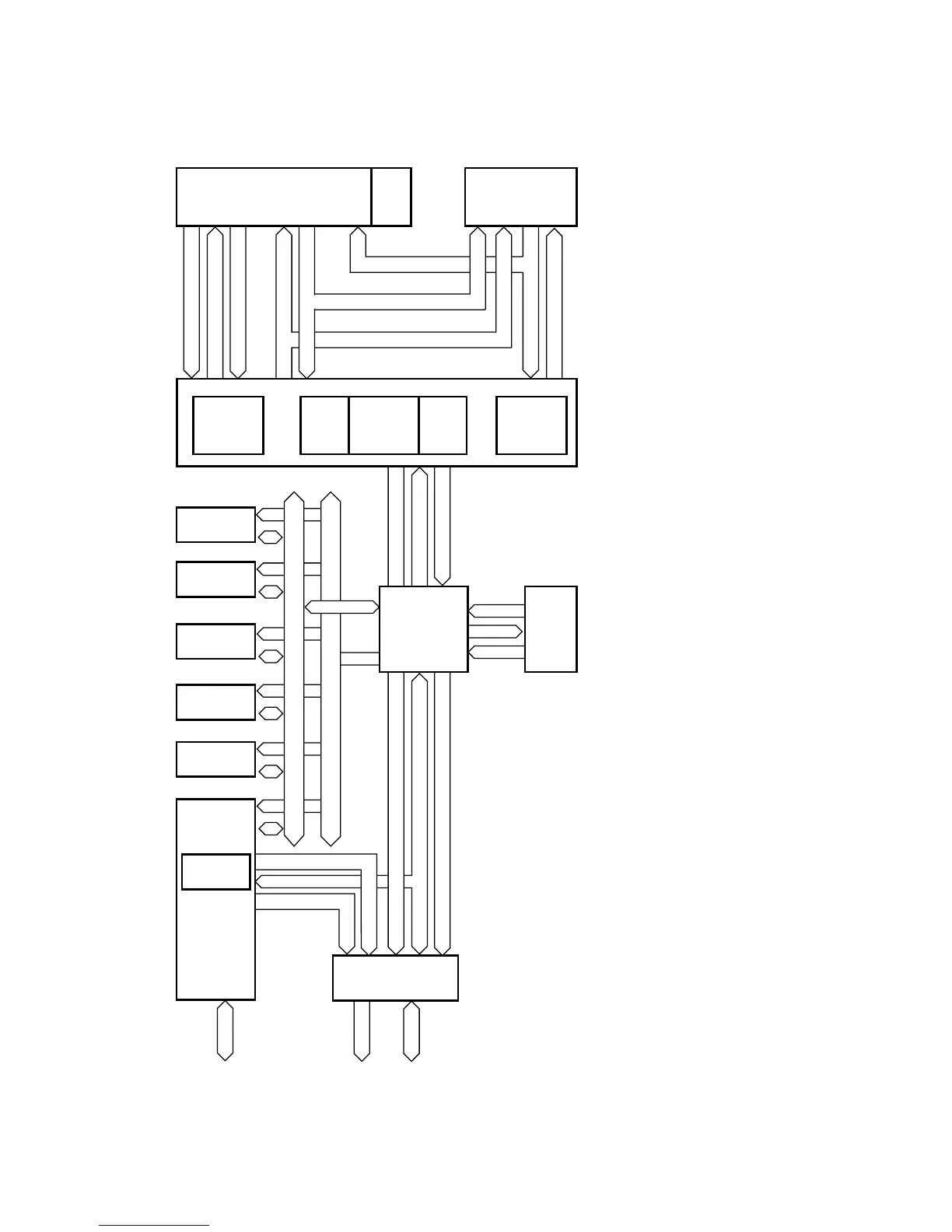
8-7-2. Block Diagram
Lower 32-bit data
64-bit data (store)
CPG
INTC
SCI
(SCIF)
RTC
TMU
External (SH) bus
interface
DMAC
32-bit data
29-bit addres
s
32-bit data
Address
32-bit data
32-bit data
Upper 32-bit data
32-bit address (instructions)
32-bit data (instructions)
32-bit address (data)
Peripheral address bus
26-bit
SH bus
address
32-bit
PCI
address/
data
32-bit
SH bus
data
Peripheral data bus
UBC
32-bit data (store)
32-bit data (load)
CPU
I cache
O cache
ITLB UTLB
Cache and
TLB
controller
FPU
BSC: Bus state controller
CPG: Clock pulse generator
DMAC: Direct memory access controller
FPU: Floating-point unit
INTC: Interrupt controller
ITLB: Instruction TLB (translation lookaside buffer)
UTLB: Unified TLB (translation lookaside buffer)
RTC: Realtime clock
SCI: Serial communication interface
SCIF: Serial communication interface with FIFO
TMU: Timer unit
UBC: User break controller
PCIC: PCI bus controller
32-bit data
PCIC
BSC
Address
(PCI)DMAC
 Loading...