95
ICE2QS01(SMPS
:IC93)
ICE2QS01BlockDiagram
Version 2.0 5 December 2006
Quasi-Resonant PWM Controller
ICE2QS01
Pin Configuration and Functionality
1 Pin Configuration and Functionality
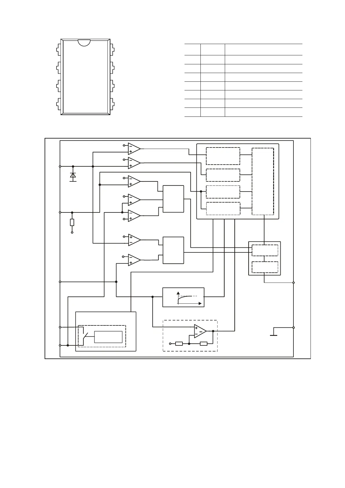
1.1 Pin Configuration
1.2 Package PG-DIP-8
Figure 1 Pin Configuration PG-DIP-8(top view)
1.3 Pin Functionality
ZC (Zero Crossing)
At this pin, the voltage from the auxiliary winding after
a time delay circuit is applied. Internally, this pin is
connected to the zero-crossing detector for switch-on
determination. Additionally, the output overvoltage
detection is realized by comparing the voltage V
zc
with
an internal preset threshold.
REG (Regulation)
Normally, an external capacitor is connected to this pin
for a smooth voltage V
reg
. Internally, this pin is
connected to the PWM signal generator for switch-off
determination (together with the current sensing
signal), the digital signal processing for the frequency
reduction with decreasing load during normal
operation, and the burst mode controller for entering
burst mode operation determination and burst ratio
control during burst mode operation. Additionally, the
open-loop / over-load protection is implemented by
monitoring the voltage at this pin.
CS (Current Sensing)
This pin is connected to the shunt resistor for the
primary current sensing, externally, and the PWM
signal generator for switch-off determination (together
with the regulation voltage), internally. Moreover, short-
winding protection is realised by monitoring the voltage
V
cs
during on-time of the main power switch.
HV (High Voltage)
The pin HV is connected to the bus voltage, externally,
and to the power cell, internally. The current through
this pin pre-charges the VCC capacitor once the supply
bus voltage is applied. Additionally, the current through
this pin supplies the IC in case that the output voltage
is lowered during active burst mode operation, or
during latch-off mode.
OUT (Gate drive output)
This output signal drives the external main power
switch, which is a power MOSFET in most case.
VCC (Power supply)
This is the IC power supply pin. Externally, this pin is
connected to the VCC capacitor, which is supplied by
the inside power cell during VCC charge-up, burst
mode operation at lowered output voltage or during
latched-off of the IC, and the auxiliary winding during
normal operation or burst mode operation with high
enough voltage across the auxiliary winding. Based on
this voltage, the VCC under- or over-voltage protection
are implemented.
GND (Ground)
This is the common ground of the controller.
Pin Symbol Function
1 ZC Zero Crossing
2 REG Regulation
3 CS Primary Current Sensing
4, 5 HV High Voltage input
6 OUT gate driver output
7 VCC IC supply voltage
8 GND Common ground
1
6
7
8
4
3
2
5
GNDZC
REG
CS
VCC
OUT
HV
HV
Quasi-Resonant PWM Controller
ICE2QS01
Representative block diagram
Version 2.0 6 December 2006
2 Representative block diagram
Figure 2 Representative Blockdigram
GND
8
CS
3
REG
2
OUT
6
ZC
1
controller
V
os
OLP
VCC
OVP
VCC
UVP
output
OVP
current limitation /
foldback correction
V
V
V
V
auto
restart
latch
off
current measurement
V
SWP
V
REF
R
ZCT2
VCCOVP
vccuvp
OPOVP
csSW
v1
power management
Reg
Vcsth
on/off FF
gate driver
PWM generator
Zero-crossing
counter
up/down
counter
HV
4, 5
VCC
7
power cell
V
OLP
active burst
control
ringing
suppression
time control
V
ZCT1
Version 2.0 5 December 2006
Quasi-Resonant PWM Controller
ICE2QS01
Pin Configuration and Functionality
1 Pin Configuration and Functionality
1.1 Pin Configuration
1.2 Package PG-DIP-8
Figure 1 Pin Configuration PG-DIP-8(top view)
1.3 Pin Functionality
ZC (Zero Crossing)
At this pin, the voltage from the auxiliary winding after
a time delay circuit is applied. Internally, this pin is
connected to the zero-crossing detector for switch-on
determination. Additionally, the output overvoltage
detection is realized by comparing the voltage V
zc
with
an internal preset threshold.
REG (Regulation)
Normally, an external capacitor is connected to this pin
for a smooth voltage V
reg
. Internally, this pin is
connected to the PWM signal generator for switch-off
determination (together with the current sensing
signal), the digital signal processing for the frequency
reduction with decreasing load during normal
operation, and the burst mode controller for entering
burst mode operation determination and burst ratio
control during burst mode operation. Additionally, the
open-loop / over-load protection is implemented by
monitoring the voltage at this pin.
CS (Current Sensing)
This pin is connected to the shunt resistor for the
primary current sensing, externally, and the PWM
signal generator for switch-off determination (together
with the regulation voltage), internally. Moreover, short-
winding protection is realised by monitoring the voltage
V
cs
during on-time of the main power switch.
HV (High Voltage)
The pin HV is connected to the bus voltage, externally,
and to the power cell, internally. The current through
this pin pre-charges the VCC capacitor once the supply
bus voltage is applied. Additionally, the current through
this pin supplies the IC in case that the output voltage
is lowered during active burst mode operation, or
during latch-off mode.
OUT (Gate drive output)
This output signal drives the external main power
switch, which is a power MOSFET in most case.
VCC (Power supply)
This is the IC power supply pin. Externally, this pin is
connected to the VCC capacitor, which is supplied by
the inside power cell during VCC charge-up, burst
mode operation at lowered output voltage or during
latched-off of the IC, and the auxiliary winding during
normal operation or burst mode operation with high
enough voltage across the auxiliary winding. Based on
this voltage, the VCC under- or over-voltage protection
are implemented.
GND (Ground)
This is the common ground of the controller.
Pin Symbol Function
1 ZC Zero Crossing
2 REG Regulation
3 CS Primary Current Sensing
4, 5 HV High Voltage input
6 OUT gate driver output
7 VCC IC supply voltage
8 GND Common ground
1
6
7
8
4
3
2
5
GNDZC
REG
CS
VCC
OUT
HV HV

 Loading...