REV.-A
2.1.3 Circuit Overview
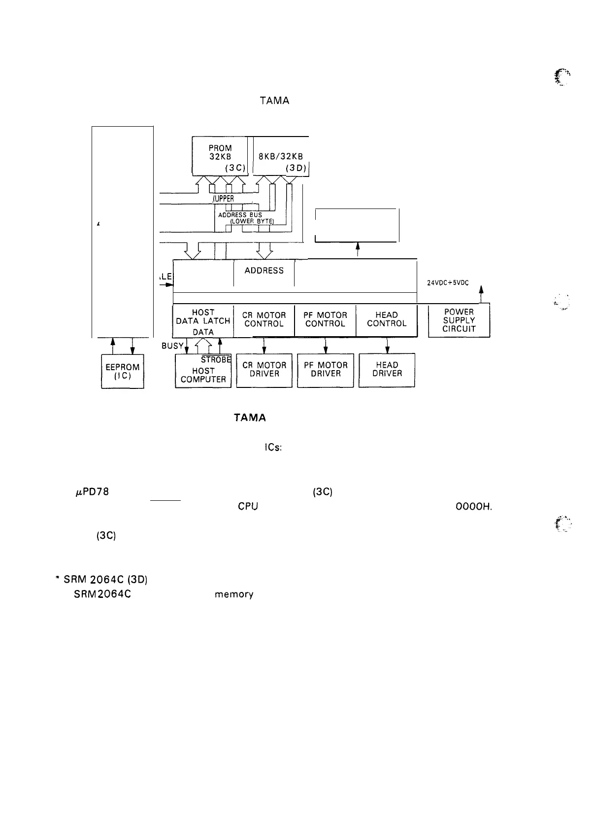
Figure 2-10 shows a block
f.
h,
,.
diagram of the TAMA board circuitry.
i
PD78 10HG
(2 c)
B
EEPROM
(1 c)
r
PROM
32KB
(3C)
RAM
8KB/32KB
h
--7rmm
‘3”)’
ADDRESS
BUS
(UPPER
BYTEI
XWl
DATA/ADDRESS BUS (LOWER BYTE)
~Q=
I
CONTROL PANEL
J
,LE
ADDRESS
A[)DRESS
CONTROL PANEL
LATCH
DECODER
LED DRIVE
+
24VDC +5VDC + 12vDC
I
I
GA E05A30 (36)
t
t
t,
‘Usir+km+=l
CG = character generator; GA = gate array.
Figure 2-10.
TAMA
Board Circuit Block Diagram
The circuit consists mainly of the following
ICS:
● ~PD7810HG CPU (2C)
The
~PD78
10HG executes the program in the PROM (3C) and controls all of the printer operations,
Upon receiving the RESET signal, the
CPIJ
begins program execution from address
OOOOH.
.
.
.
.
.
.
<-.,’.,
● PROM (3C)
The PROM includes the control program (firmware) and character generators.
“
SRM
2064C
(3D)
The
SRM
2064C
SRAM is external melmory for the CPU. It is used as an input data buffer and line buffer
for expanding data, and as working area for the program.
2-8
 Loading...