Table 14 (Cont.)
Description of Function Block
Function Block Name Function
DPDC#B Digital Pre-Distortion
Central unit#B
▪ DPDC#B has a Power Supply (PS) function for the RU. It has a
DPD and CFR control function for PA of n70n66-RF#B.
n70n66-RF n70n66-RF#A
n70n66-RF#B
▪ A transmission RF signal from the RF-IC is amplied by a power
amplier (PA) for each band.
▪ A received RF signal from a duplexer is amplied by a Low Noise
Amplier (LNA).
▪ Transmission digital signal from TRX is converted into a
transmission RF signal aer performing D/A conversion and
orthogonal modulation at RF-IC and Received RF signal from a
duplexer is demodulated and A/D converted, and the received
digital signal is an output to TRX.
DUP Duplexer ▪ e RF signals of each frequency bands (n70, n66) are combined
and separated, and the frequency bands of the transmied RF
signal and the received RF signal are passed and the out-of-band
components are removed.
PS Power Supply ▪ Provides necessary power voltage to the RU from a DC power
supply input (DC-36.0 V…–58.0 V).
TRX Transmier and Receiver ▪ It has a high-speed data (baseband signals) interface of LLB. It
also has an interface with the Radio Frequency Integrated Circuit
(RFIC), to perform DPD and CFR processing of the transmission
signal and Digital Down Conversion (DDC) processing of the
received RF signal.
LLB Lower Layer Baseband ▪ IQ signals in Lower Layer Split (LLS) and monitoring signals are
transmied between a higher NR system CU device and TRX by
an optical ber according to an eCPRI format.
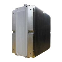
RU Hardware Feature
Functional Block Diagram
54
Release 1.0 · Issue 1.1, May 2021
Fujitsu and Fujitsu Customer Use Only