2.6
Functional Block Diagram
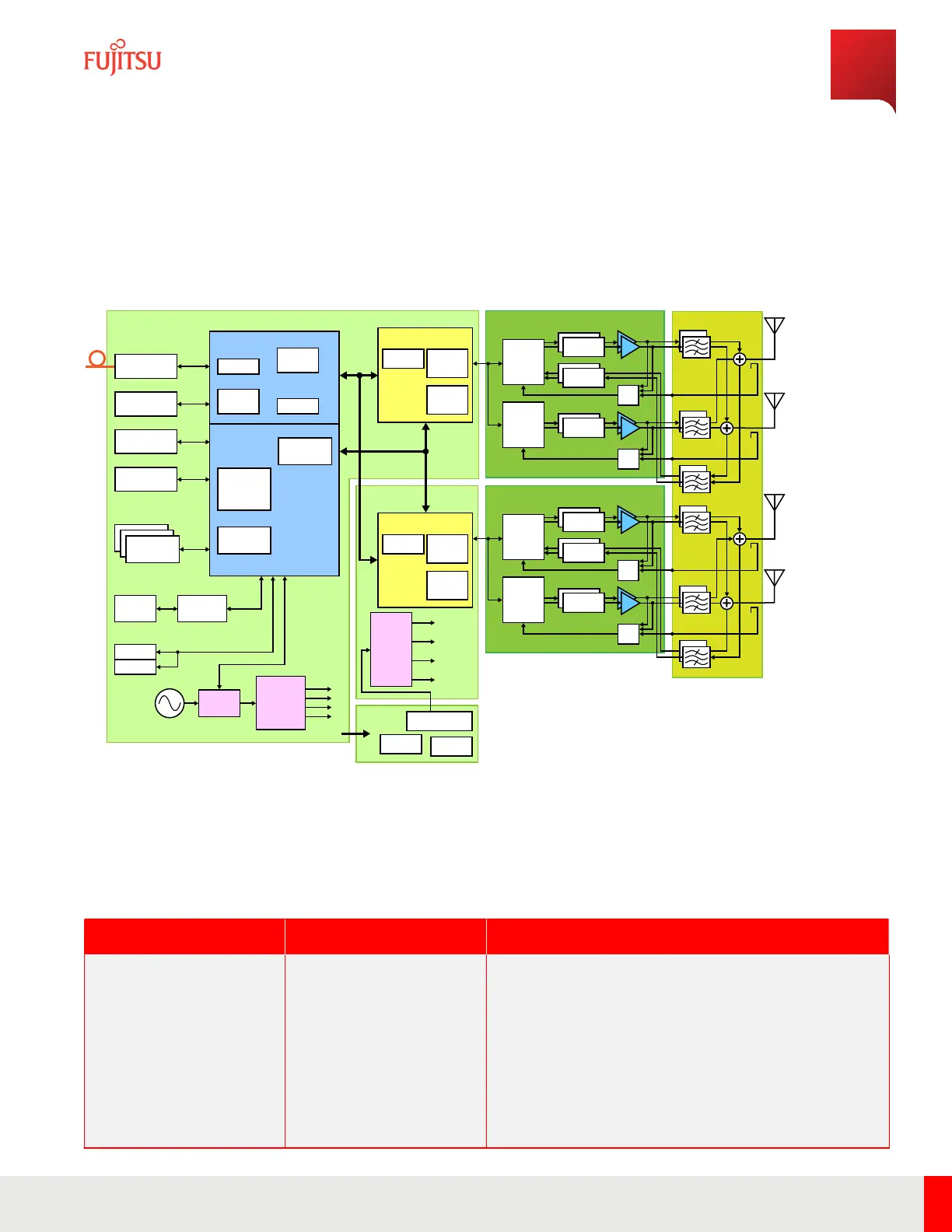
e following gure shows a functional diagram of the RU.
DPDC#A
DPDC#B
PS
PL
TRX#1
TRX#2
PS
n70n66-RF#A
DUP
Opt Module
(10G)
Serdes
CFR
DPD
TXCONV
PA
PATXCONV
RXCONV
RF-IC
2T2R
n70
RF-IC
2T2R
n66
Rx
DDC
CFR
HOT&SWAP
Surge
EMI-Fil
DPD
Rx
DDC
RACH
PHY
MAC
MPU
(Multi-
Core)
iFFT
FFT
Bus
Controller
Memory
Controller
SRAM
I2C
Hi Speed
PCI-e
JESD
RVS#A
RVS#C
RVS#B
ANT
#D
ANT
#B
ANT
#C
ANT
#A
RVS#D
40W
60W
RF-SW
RF-SW
n70n66-RF#B
TXCONV
PA
PATXCONV
RXCONV
RF-IC
2T2R
n70
RF-IC
2T2R
n66
JESD
40W
60W
RF-SW
RF-SW
QSPI
DDR-JF
Work Memory
+E
CC
1000BASE-T
RGMII SPI
CLK
-48V
+53V, +12V
DPRF#A
+53V, +12V
DPRF#B
DPDC
+12V
DPDC
(AISG)
+24V
EEPROM
QSPI-FLASH
DDR4
RJ45
CN
LAN-PHY
LED
AISG
PTP
De
vice
PS
Jitter
Cleaner
PPL
FNC001698_Rev_01
Figure 5
Functional Diagram
Table 14
Description of Function Block
Function Block Name Function
DPDC#A Digital Pre-Distortion
Central unit#A
▪ DPDC#A monitors and controls each interface in the RU by LLB. It
has a Digital Pre-Distortion (DPD) and Crest Factor Reduction
(CFR) control function for PA of n70n66-RF#A.
▪ e eCPRI block in the LLB has a Serdes interface with the optical
module and a PHY/MAC unit that constructs the frame format of
the C/U/S/M-Plane.
▪ e iFFT/FFT block performs IQ conversion/inverse conversion of
the uplink ad downlink U-planes.
▪ e RACH Block is a processing function for the random access
channel.
RU Hardware Feature
Functional Block Diagram
53
Release 1.0 · Issue 1.1, May 2021
Fujitsu and Fujitsu Customer Use Only