Cinterion
®
LTE Terminals Hardware Interface Description
8.5 Configuring GPIO Directions
101
ELSxT_HID_v04 2018-09-04
Confidential / Preliminary
Page 94 of 102
8.5.2 Configuration using TXD0 Line of ASC0 Interface
Please refer to Section 8.3 for more information on how to configure the watchdog via TXD0
line of ASC0 interface.
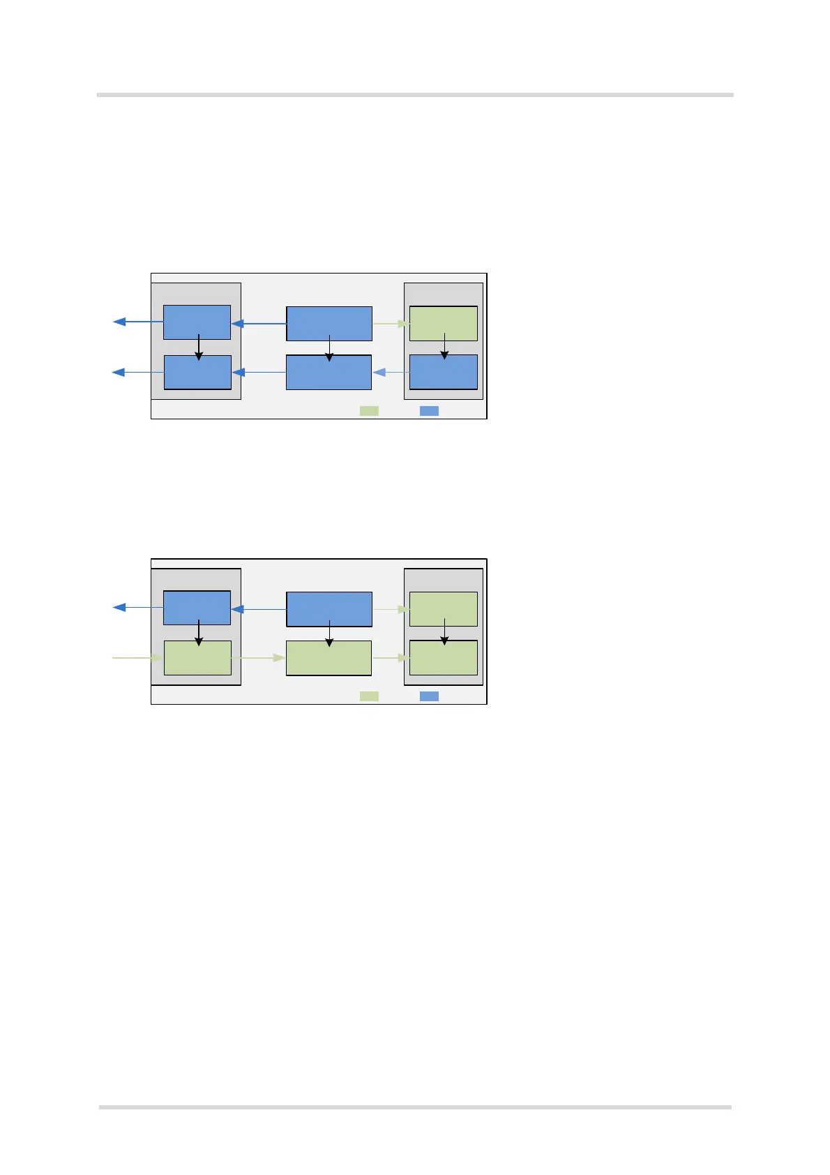
Figure 30 explains the configuration steps required to set the LTE Terminals‘s GPIO7 signal
direction to OUTPUT (default direction is INPUT):
Figure 32: Setting GPIO direction to OUTPUT via TXD0 line (at 1200bps)
Figure 30 shows the configuration steps required to re-set the LTE Terminal‘s GPIO7 signal
direction to INPUT:
Figure 33: Setting GPIO direction to INPUT via TXD0 line (at 1200bps)
For more information on the AT commands mentioned in the above figures see also [1].
GPIO connector Java module
Level shifter
GPIO7
GPIO7
Set level shifter to OUTPUT with watchdog
command WD=GPIO_DIR,527,14 *
Level shifter
GPIO7
GPIO7
Set GPIO7 at Java module to OUTPUT with
GPIO command AT^SCPIN=1,6,1
Now, IO state can be set with AT^SSIO=6,0
Steps:
Voltage level conversion
Java Terminal
= INPUT
= OUTPUT
* See Section 8.3.1.11 for configuration details.
GPIO connector Java module
Level shifter
GPIO7
GPIO7
Set level shifter to INPUT with watchdog
command WD=GPIO_DIR,525,12 *
Now, GPIO7 can be read out with AT^SGIO=6
Level shifter
GPIO7
GPIO7
Set GPIO7 at Java module to INPUT with
GPIO command AT^SCPIN=1,6,0
Steps:
Voltage level conversion
Java Terminal
= INPUT
= OUTPUT
* See Section 8.3.1.11 for configuration details.
 Loading...