GD-Link V2 Adapter User Guide
6
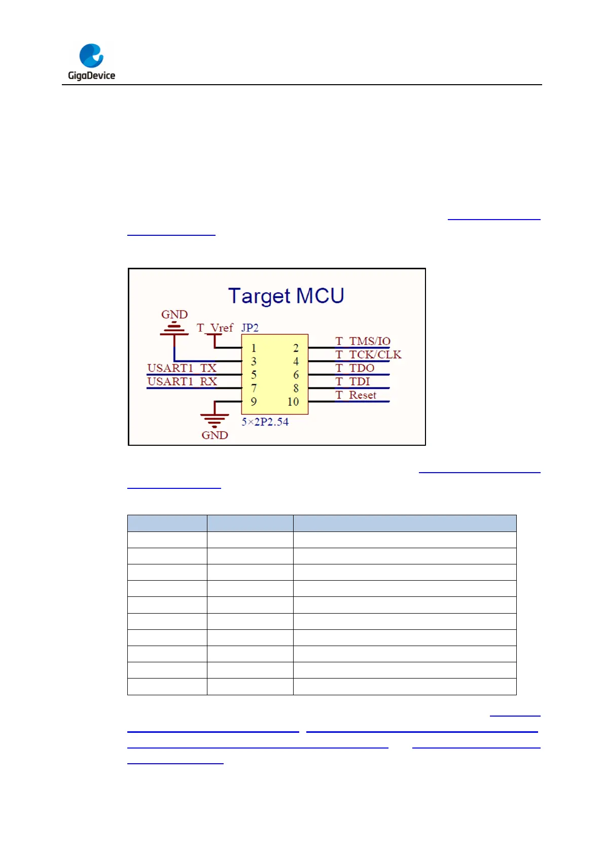
2. Hardware introduction
2.1. Pin definitions and wiring methods
To enable programming, debugging, serial communication, and printing functions, connect
the GD-Link V2 pins to the SWD (SWO), JTAG, or USART interface of the target chip using
DuPont wires or ribbon cables. The pinout of GD-Link V2 is illustrated in Figure 2-1. GD-Link
V2 pinout diagram.
Figure 2-1. GD-Link V2 pinout diagram
The functions of each GD-Link V2 pin are described as shown in Table 2-1. GD-Link V2 pin
function definitions.
Table 2-1. GD-Link V2 pin function definitions
Target chip power supply, providing 3.3V / 5V
JTAG TMS pin / SWD SWDIO pin
JTAG TCK pin / SWD CLK pin
JTAG / SWD target chip reset pin
The diagram of GD-Link V2 hardware connection to the target chip is illustrated in Figure 2-2.
SWD interface connection diagram, Figure 2-3. JTAG interface connection diagram,
Figure 2-4. SWD + SWO interface connection diagram and Figure 2-5. Serial interface
connection diagram.