Rev. 1.50 72 August 28, 2017 Rev. 1.50 73 August 28, 2017
HT66F0175/HT66F0185
A/D Flash MCU with EEPROM
HT66F0175/HT66F0185
A/D Flash MCU with EEPROM
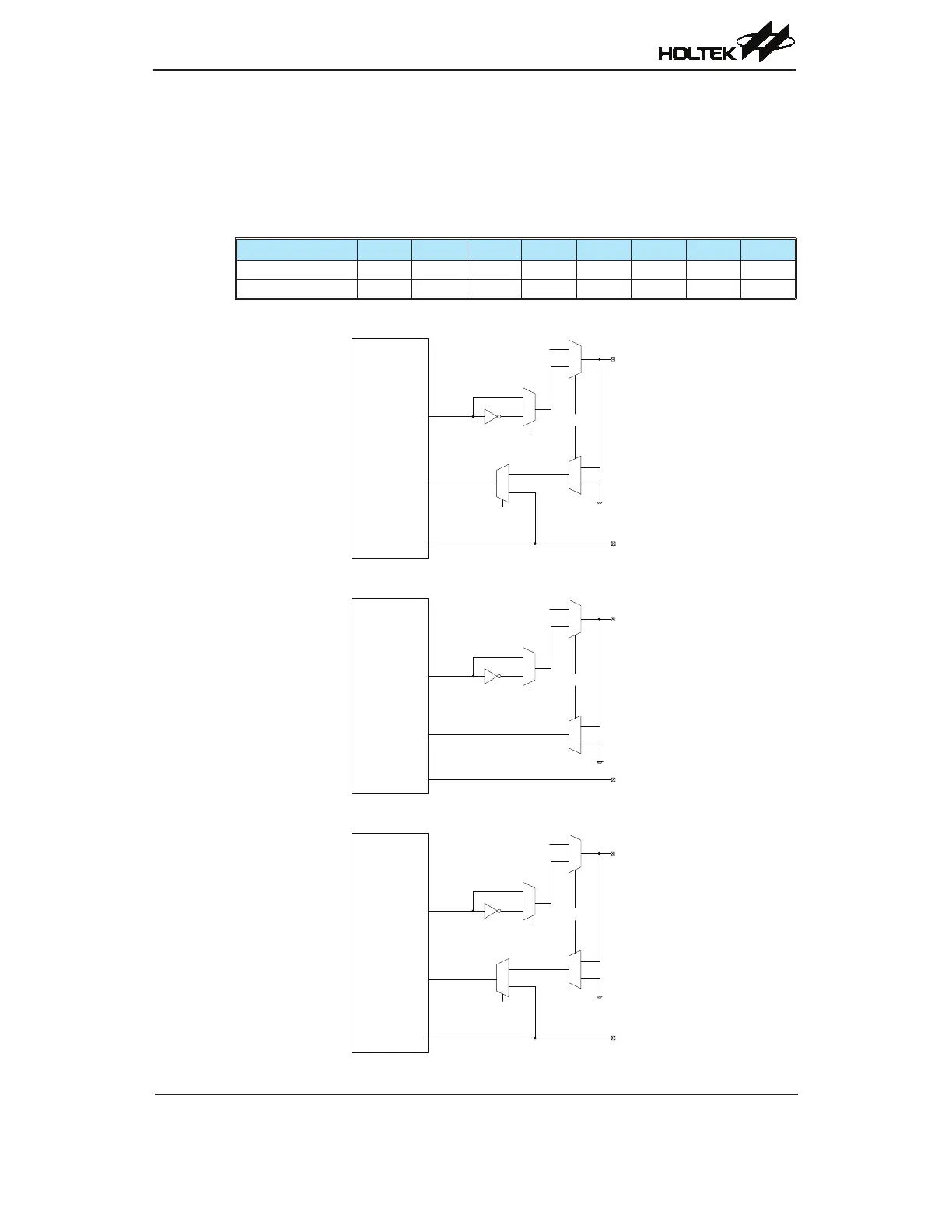
TM Input/Output Pin Control Register
SelectingtohaveaTMinput/outputorwhethertoretainitsothersharedfunctionisimplemented
usingtherelevantpin-sharedfunctionselectionregisters,withthecorrespondingselectionbitsin
eachpin-sharedfunctionregistercorrespondingtoaTMinput/outputpin.Conguringtheselection
bitscorrectlywillsetupthecorrespondingpinasaTMinput/output.Thedetailsofthepin-shared
functionselectionaredescribedinthepin-sharedfunctionsection.
Register Name Bit7 Bit6 Bit5 Bit4 Bit3 Bit2 Bit1 Bit0
TMPC (HT66F0175) CLOP — — — — — T1CP T0CP
TMPC (HT66F0185) CLOP — — — — T2CP T1CP T0CP
TM Pin Control Register List
TM0
(PTM)
PA0/TP0
T0CP
PA0 Output Function
0
1
Output
Capture Input
T0CAPTS
PB2/TCK0
TCK Input
0
1
PA0
0
1
1
0
TM0 Function Pin Control Block Diagram – HT66F0175 only
TM0
(STM)
PA0/TP0
T0CP
PA0 Output Function
0
1
Output
Capture Input
PB2/TCK0
TCK Input
0
1
PA0
1
0
TM0 Function Pin Control Block Diagram – HT66F0185 only
TM1
(PTM)
PA7/TP1
T1CP
PA7 Output Function
0
1
Output
Capture Input
T1CAPTS
PA4/TCK1
TCK Input
0
1
PA7
0
1
1
0
TM1 Function Pin Control Block Diagram – HT66F0175/HT66F0185