Rev. 1.50 74 August 28, 2017 Rev. 1.50 75 August 28, 2017
HT66F0175/HT66F0185
A/D Flash MCU with EEPROM
HT66F0175/HT66F0185
A/D Flash MCU with EEPROM
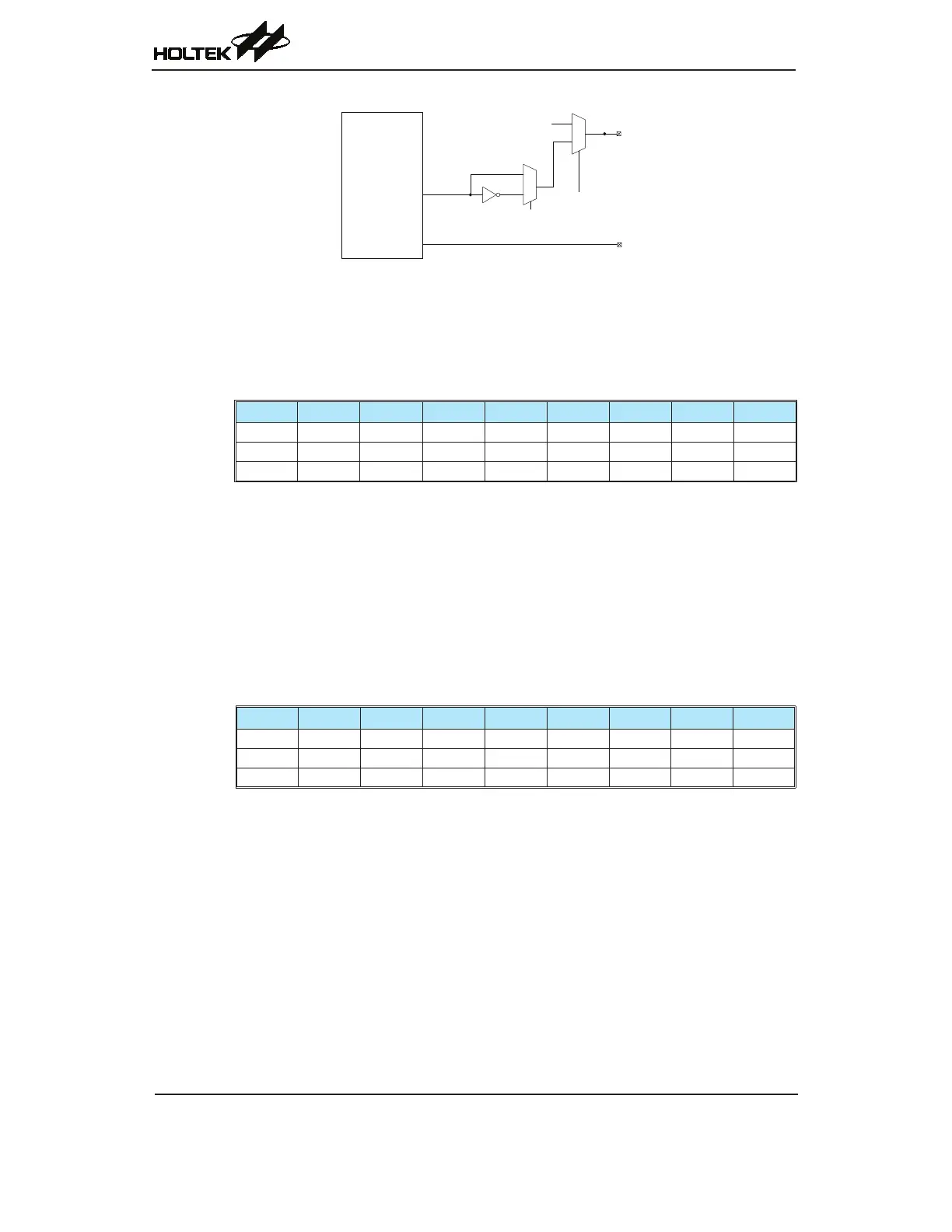
TM2
(CTM)
PB3/TP2
T2CP
PB3 Output Function
0
1
Output
PA6/TCK2
TCK Input
0
1
PB3
TM2 Function Pin Control Block Diagram – HT66F0185 only
Note:1.TheI/OregisterdatabitsshownareusedforTMoutputinversioncontrol.
2.IntheCaptureInputMode,theTMpincontrolregistermustneverenablemorethanone
TMinput.
TMPC Register – HT66F0175
Bit 7 6 5 4 3 2 1 0
Name CLOP — — — — — T1CP T0CP
R/W R/W — — — — — R/W R/W
POR 0 — — — — — 0 0
Bit7 CLOP:CLOpincontrol
0:Disable
1:Enable
Bit6~2 Unimplemented,readas“0”
Bit1 T1CP:TP1pincontrol
0:Disable
1:Enable
Bit0 T0CP:TP0pincontrol
0:Disable
1:Enable
TMPC Register – HT66F0185
Bit 7 6 5 4 3 2 1 0
Name CLOP — — — — T2CP T1CP T0CP
R/W R/W — — — — R/W R/W R/W
POR 0 — — — — 0 0 0
Bit7 CLOP:CLOpincontrol
0:Disable
1:Enable
Bit6~3 Unimplemented,readas“0”
Bit2 T2CP:TP2pincontrol
0:Disable
1:Enable
Bit1 T1CP:TP1pincontrol
0:Disable
1:Enable
Bit0 T0CP:TP0pincontrol
0:Disable
1:Enable