Service Manual UHF2 (450-520MHz) Information
121
8. UHF2 (450-520MHz) Information
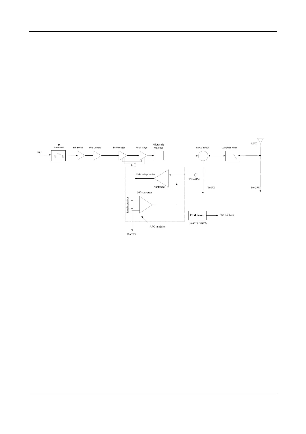
8.1 Transmitter Circuit
The transmitter circuit is mainly composed of:
RF power amplifier circuit
Low-pass filter circuit (for suppressing harmonics)
Auto power control circuit (APC) (including temperature detection circuit)
Figure 8-1 Diagram of Transmitter Circuit
8.1.1 RF Power Amplifier Circuit
The carrier signal generated by the TX VCO is modulated and amplified, and then feeds to the
transmitter circuit via the following steps.
Step 1 The signal passes through a π-type attenuator first, allowing interstage isolation between the
RF power amplifier circuit and TX VCO.
Step 2 The signal goes to a pre-driver amplifier (2SC3356) for pre-amplification, providing further
interstage isolation.
Step 3 The signal goes to another pre-driver amplifier (2SC4988) and a driver amplifier (RD01) for
adequate power amplification, so as to obtain further amplification in the final-stage amplifier
(RD07).
 Loading...