UHF1 (400-470MHz) Information Service Manual
36
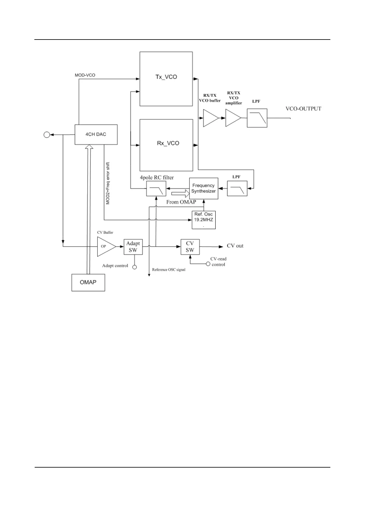
Figure 7-4 Diagram of FGU
7.3.1 Working Principle of PLL
The 19.2MHz frequency generated by the reference crystal oscillator goes to PLL for division,
generating the reference frequency (i.e. step frequency f1). Meanwhile, the frequency generated by
VCO generates another frequency (f2) through the frequency divider in PLL. Then frequencies f1 and f2
are compared in the phase detector (PD), to generate continuous pulse current. The current goes to the
loop filter for RC integration, and is then converted to CV voltage. Then the CV voltage is sent to the
varactor of VCO. It adjusts the output frequency of VCO directly until the CV voltage becomes constant.
Then the PLL is locked, and the stable frequency output by VCO goes to the TX-RX channel after
passing through two buffer amplifiers.
 Loading...