Home
Hytera
Portable Radio
PD78XG
Hytera PD78XG Service Manual
5
of 1
of 1 rating
513 pages
Give review
Manual
Specs
To Next Page
To Next Page
To Previous Page
To Previous Page
Loading...
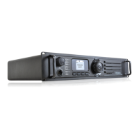
Service Manual
Interface
Definition
31
No.
OPT_SEL1
OPT_SEL2
OPT_SEL3
Definition
5
1
0
0
For connecting MODEM
6
1
0
1
For connecting remote speaker microphones
7 1
1
0
Programming cable (serial port)/
USB slave mode for the radio
8 1
1
1
No
accessory
Table 6-6 Definition of Accessory Identifiers
40
42
Table of Contents
Default Chapter
4
Table of Contents
4
Documentation Information
11
1 Introduction
12
2 Product Controls
13
3 Baseband Section
16
Power Section
16
Diagram of Power Control
16
Radio On/Off
16
Figure 3-1 Diagram of Power Control
16
Figure 3-2 Diagram of Radio On/Off Control
16
Power Protection
17
Power Consumption Control
17
Control Section
17
OMAP5912 Dual-Core Processor
17
Figure 3-3 Diagram of OMAP5912
18
Figure 3-4 Diagram of Overall Scheme
18
External Memory
19
Figure 3-5 Diagram of External Memory
19
Clock
20
Figure 3-6 Diagram of Baseband Clock
20
Reset Signal
21
Spi
21
Mcbsp
21
Figure 3-7 Diagram of Reset Signal
21
Figure 3-8 Diagram of SPI Connection
21
Usb
22
Figure 3-9 Diagram of MCBSP Connection
22
Figure 3-10 Diagram of USB Interface
22
Uart
23
I2C
23
Figure 3-11 Diagram of UART Interface Connection
23
Figure 3-12 Diagram of I2C Connection
23
Microwire
24
Mcsi1
24
Audio Section
24
Audio Diagram
24
Figure 3-13 Diagram of MICROWIRE Connection
24
Figure 3-14 Diagram of MCSI1 Connection
24
Diagram of Signal Flow
25
Figure 3-15 Diagram of Audio Section
25
Audio Amplifier
26
Figure 3-16 Diagram of Audio Signal Flow
26
Troubleshooting Flow Chart
27
PCB Difference
28
4 GPS Circuit
29
Circuit Description
29
Figure 4-1 Diagram of GPS Circuit
29
Schematic Diagram
30
Parts List
30
Figure 4-2 Schematic Diagram
30
Troubleshooting Flow Chart
33
5 Tuning Description
34
6 Interface Definition
35
Table 6-1 Definition of 50-Pin Interface
37
Table 6-2 Definition of 30-Pin LCD Interface
37
Table 6-3 Definition of Channel Board Interface
38
Table 6-4 Definition of 20-Pin Option Board Interface
40
Table 6-5 Definition of 16-Pin Accessory Interface
40
Table 6-6 Definition of Accessory Identifiers
41
7 UHF1 (400-470Mhz) Information
42
Transmitter Circuit
42
RF Power Amplifier Circuit
42
Figure 7-1 Diagram of Transmitter Circuit
42
Low-Pass Filter Circuit
43
Auto Power Control Circuit
43
Receiver Circuit
43
Receiver Front-End
44
Figure 7-2 Diagram of Receiver Circuit
44
Receiver Back-End
45
Frequency Generation Unit (FGU)
45
Figure 7-3 Diagram of if Processor
45
Figure 7-4 Diagram of FGU
46
Working Principle of PLL
46
Two-Point Modulation
47
Working Principle of VCO
47
PCB View
48
Block Diagram
56
Schematic Diagram
59
Parts List
75
Troubleshooting Flow Chart
125
8 UHF2 (450-520Mhz) Information
131
Transmitter Circuit
131
RF Power Amplifier Circuit
131
Figure 8-1 Diagram of Transmitter Circuit
131
Low-Pass Filter Circuit
132
Auto Power Control Circuit
132
Receiver Circuit
132
Receiver Front-End
133
Figure 8-2 Diagram of Receiver Circuit
133
Receiver Back-End
134
Frequency Generation Unit (FGU)
134
Figure 8-3 Diagram of if Processor
134
Figure 8-4 Diagram of FGU
135
Working Principle of PLL
135
Working Principle of VCO
135
Two-Point Modulation
136
PCB View
137
Block Diagram
145
Schematic Diagram
148
Parts List
164
Troubleshooting Flow Chart
215
9 UHF3 (350-400Mhz) Information
221
Transmitter Circuit
221
RF Power Amplifier Circuit
221
Figure 9-1 Diagram of Transmitter Circuit
221
Low-Pass Filter Circuit
222
Auto Power Control Circuit
222
Receiver Circuit
222
Receiver Front-End
223
Figure 9-2 Diagram of Receiver Circuit
223
Receiver Back-End
224
Frequency Generation Unit (FGU)
224
Figure 9-3 Diagram of if Processor
224
Figure 9-4 Diagram of FGU
225
Working Principle of PLL
225
Working Principle of VCO
225
Two-Point Modulation
226
PCB View
227
Block Diagram
235
Schematic Diagram
238
Parts List
254
Troubleshooting Flow Chart
305
10 UHF5 (806-941Mhz) Information
311
Transmitter Circuit
311
RF Power Amplifier Circuit
311
Figure 10-1 Diagram of Transmitter Circuit
311
Low-Pass Filter Circuit
312
Auto Power Control Circuit
312
Receiver Circuit
312
Receiver Front-End
313
Figure 10-2 Diagram of Receiver Circuit
313
Receiver Back-End
314
Frequency Generation Unit (FGU)
314
Figure 10-3 Diagram of if Processor
314
Figure 10-4 Diagram of FGU
315
Working Principle of PLL
315
Working Principle of VCO
315
Two-Point Modulation
316
PCB View
317
Block Diagram
325
Schematic Diagram
328
Parts List
344
Troubleshooting Flow Chart
398
11 VHF (136-174Mhz) Information
406
Transmitter Circuit
406
RF Power Amplifier Circuit
406
Figure 11-1 Diagram of Transmitter Circuit
406
Low-Pass Filter Circuit
407
Auto Power Control Circuit
407
Receiver Circuit
407
Receiver Front-End
408
Figure 11-2 Diagram of Receiver Circuit
408
Receiver Back-End
409
Frequency Generation Unit (FGU)
409
Working Principle of PLL
410
Working Principle of VCO
410
Direct Modulation
411
PCB View
412
Block Diagram
420
Schematic Diagram
423
Parts List
439
Troubleshooting Flow Chart
492
12 Disassembly and Assembly
498
Disassembling the Chassis
498
Disassembling the TX and RX Units
498
Assembly
499
13 Exploded View
500
14 Packing Guide
506
15 Specifications
507
16 Appendix
510
Table 16-1 UHF1 Blind Spot
511
Table 16-2 UHF2 Blind Spot
511
Table 16-3 UHF3 Blind Spot
512
Table 16-5 VHF Blind Spot
512
Other manuals for Hytera PD78XG
Manual
42 pages
System Planner
182 pages
Owner's Manual
15 pages
User Manual
35 pages
5
Based on 1 rating
Ask a question
Give review
Questions and Answers:
Need help?
Do you have a question about the Hytera PD78XG and is the answer not in the manual?
Ask a question
Hytera PD78XG Specifications
General
Brand
Hytera
Model
PD78XG
Category
Portable Radio
Language
English
Related product manuals
Hytera PD78X
42 pages
Hytera PD78X Series
182 pages
Hytera PD785
41 pages
Hytera PD782i
17 pages
Hytera PD705
27 pages
Hytera PD702
17 pages
Hytera PD708
17 pages
Hytera PD706
17 pages
Hytera PD706G
17 pages
Hytera PD705LT
17 pages
Hytera PD795 Ex
31 pages
Hytera PD79 Ex Series
31 pages