Service Manual UHF1 (400-470MHz) Information
35
7.2.2 Receiver Back-end
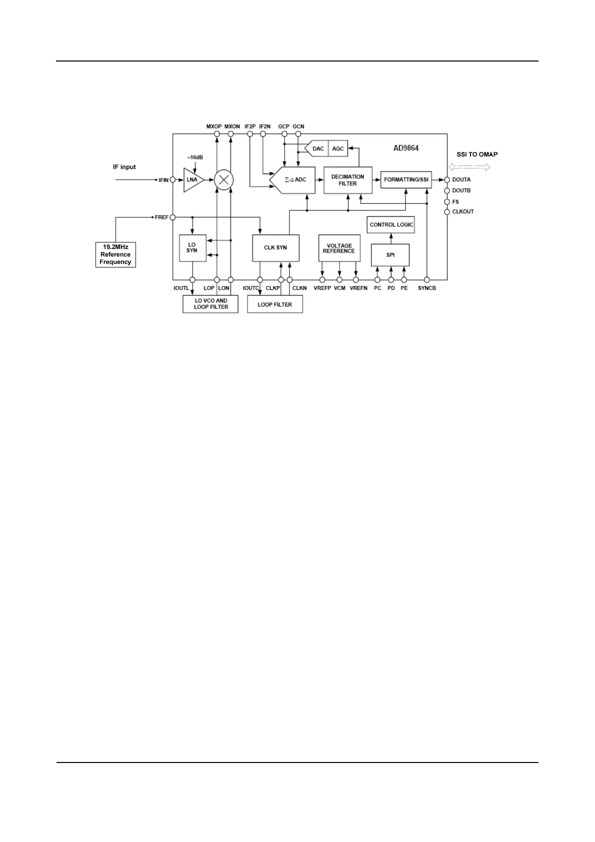
Figure 7-3 Diagram of IF Processor
The first IF signal (73.35MHz) output by the IF amplifier goes into AD9864 (U401) via Pin 47, where the
signal is converted to the second IF signal (2.25MHz). Then the signal is converted to digital signal via
ADC sampling, and output via the SSI interface. Finally, the digital signal is sent to DSP (OMAP5912) for
demodulation.
AD9864 employs reference frequency of 19.2MHz and shares the crystal with the OMAP. The second
LO VCO comprises an oscillator, a varactor and some other components, to provide the 71.1/75.6MHz
LO signal. The 18MHz clock frequency is generated by the LC resonance loop.
7.3 Frequency Generation Unit (FGU)
The FGU is composed of VCO and PLL. It is the core module of the whole TX-RX system. This circuit
provides accurate carrier frequency during transmission, and stable LO signal during reception. It has a
direct influence on the performance of the system.
 Loading...