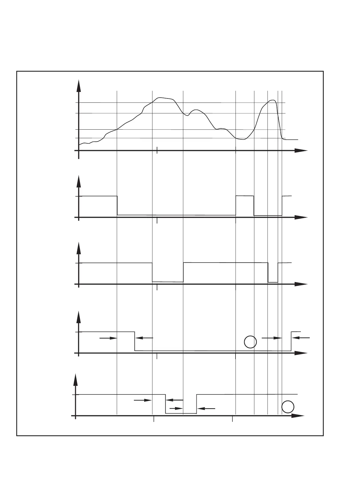
26
13.2 Switching delay for the upper limit monitor
The time diagram shows the effect of the switching delay on the analogue input
for an upper limit monitor (ESP1 < ESP2)� The outputs are set as normally closed
(OU1 and OU2 → NC).
2
t [s]
10
20
Analogue In
[°C]
ESP2
ESP1
t [s]
10
20
OU 1 (n.c.)
ds1, ds2, dr1, dr2 = 0 s
24 V
0 V
on
off
off
on
t [s]
10
20
OU 2 (n.c.)
24 V
0 V
on
off
off
on
t [s]
10
20
OU 1 (n.c.)
ds1, ds2 = 2 s / dr1, dr2 = 3 s
24 V
0 V
on
off
2 s
3 s
t [s]
10
20
OU 2 (n.c.)
ds1, ds2 = 2 s / dr1, dr2 = 3 s
24 V
0 V
off
2 s
3 s
1
on
Eh2
{
Eh1
{
1: Not switched off because the selected switching delay is too short (< 3 s)�
2: Not switched on because the selected switching delay is too short (< 2 s)�