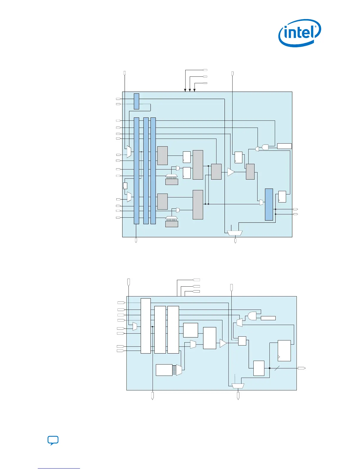
Figure 2. Fixed-Point Arithmetic 18 x 19 Mode
Pipleine Register
Input Register Bank
scanin[18..0]
scanout[18..0]
LOADCONST
ACCUMULATE
NEGATE
ay[18..0]
az[17..0]
ax[17..0]
COEFSELA[2..0]
by[18..0]
bz[17..0]
bx[17..0]
COEFSELB[2..0]
SUB
+/-
Pre-Adder
+/-
Pre-Adder
+/-
Internal
Coefficient
Internal
Coefficient
Multiplier
Adder
and Subtractor
+/-
+/-
**Systolic
Registers
**Systolic
Register
Chainout adder/
accumulator
+
Output Register Bank
Double
Accumulation
Register
chainin[63..0]
chainout[63..0]
resulta[36:0]
Multiplier
x
x
CLK
ENA[2..0]
CLR[1..0]
**Systolic registers are enabled in systolic mode only.
*1st Pipleine Register
resultb[36:0]
*2nd Pipleine Register
*This block diagram shows the functional representation of the DSP block. The pipeline registers are embedded within the various circuits of the DSP block.
**Systolic
Registers
0
1
1 0
DISABLE_CHAINOUT
DISABLE_SCANIN
Top delay
register
64’b0
Input Register
Constant
Figure 3. Fixed-Point Arithmetic 27 x 27 Mode
Constant
64
Double
Accumulation
Register
resulta[63:0]
chainout[63:0]
Internal
Coefficients
+/-
LOADCONST
ACCUMULATE
NEGATE
ay[26:0]
az[25:0]
ax[26:0]
COEFSELA[2:0]
Multiplier
x
chainin[63:0]
Output
Register
Bank
Chainout Adder/
Accumulator
Input
Register
Bank
Pre-Adder
+/-
*1st
Pipeline
Register
*2nd
Pipeline
Register
scanin[26:0]
scanout[26:0]
*This block diagram shows the functional representation of the DSP block. The pipeline registers are embedded within the various circuits of the DSP block.
clk
ena[2:0]
clr [1:0]
+
64’b0
1
0
DISABLE_CHAINOUT
2. Intel Agilex Variable Precision DSP Blocks Architecture
UG-20213 | 2019.04.02
Send Feedback
Intel
®
Agilex
™
Variable Precision DSP Blocks User Guide
11
 Loading...