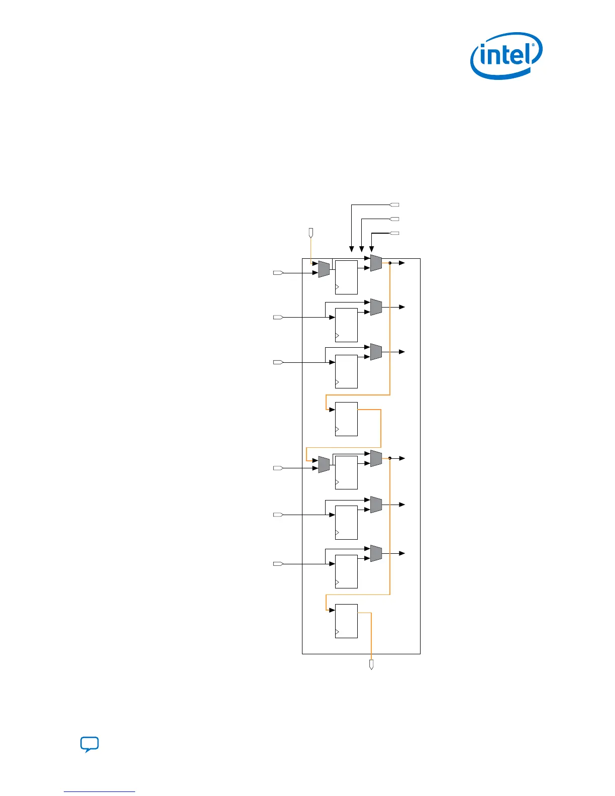
input register must be enabled when top delay register is enabled. The clock enable
for both registers must be the same. Similarly, the by input register must be enabled
when bottom delay register is enabled. The clock enable for both registers must be
the same.
The delay registers are only supported in 18 x 18 or 18 x 19 independent multiplier,
multiplier adder sum mode and 18-bit systolic FIR mode.
Figure 47. Input Cascade in Fixed-Point Arithmetic 18 x 19 Mode
ay[18..0]
az[17..0]
ax[17..0]
by[18..0]
Top delay registers
bz[17..0]
bx[17..0]
Bottom delay registers
scanin[18..0]
scanout[18..0]
CLK
ENA[2..0]
CLR[0]
4. Intel Agilex Variable Precision DSP Blocks Design Considerations
UG-20213 | 2019.04.02
Send Feedback
Intel
®
Agilex
™
Variable Precision DSP Blocks User Guide
65