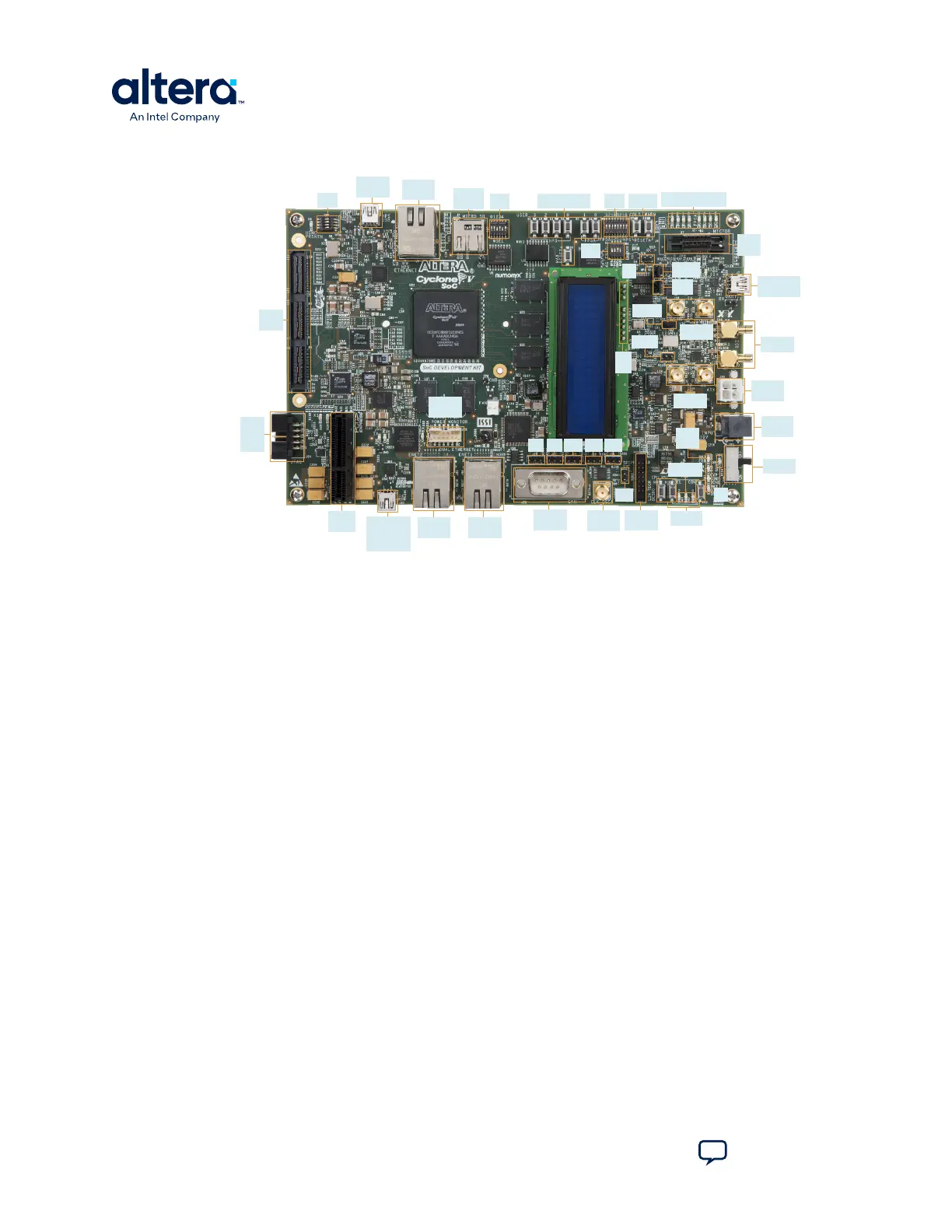
Figure 19. Components in Cyclone V SoC Development Kit (Power Solution 1)—Top View
LEDs
(D1, D2, D3, D4, D5, D6, D7, D8)
DIP Switches
(S7, S8)
Switch
(SW1)
DIP Switches
(S1, S2, S3, S4, S5, S6, S9)
Switch
(SW3)
Micro SD Card
Connector
(J3)
RJ45 Connector
for HPS
(J2)
Micro USB
Connector
(J1)
Switch
(SW2)
HSMC
Connector
(J12)
External
Download
Cable JTAG
Header
(J23)
PCI Express*
Connector
(J25)
2x6 Header for
Power Monitor
(J24)
Mini USB Connector
for Onboard
Intel® FPGA
Download Cable
(J37)
RJ45
Connector 2
(J33)
RJ45
Connector 1
(J34)
D-Sub
Connector
(J35)
SMA
Connector
(J36)
2x7 Header
for HPS
(J32)
DIP Switches
(S10, S11, S12)
Power Switch
(SW5)
SMB Connector
(J14, J17)
Power Adapter
Input
(J22)
ATX Power
Input
(J20)
SMB Connector
(J10, J11)
SMB Connector
(J18, J19)
Mini USB Connector
for UART
(J8)
LCD
Header
(J15)
Mictor
Connector
(J4)
LEDs
(D39, D40, D41)
LEDs
(D34, D36,
D37, D38)
Switch
(SW4)
9V
(J5)
JTAG HPS SEL
(J6)
JTAG SEL
(J7)
LED
(D35)
CLKSEL0
(J26)
CLKSEL1
(J27)
BOOTSEL0
(J28)
BOOTSEL1
(J29)
BOOTSEL2
(J30)
SPI I2C
(J31)
OSC1_CLK_SEL
(J13)
JTAG MIC SEL
(J16)
A.2. Programming Flash Memory
This appendix describes programming information for the following memory devices:
• Common flash interface (CFI) flash memory
• Quad serial peripheral interface (quad SPI) flash memory
• SD card flash memory
The Cyclone V development board's flash memory ships preconfigured with the
parallel flash loader (PFL) option bits to support FPGA designs to be written to any of
the three locations as shown in the Byte Address Flash Memory Map table. The PFL is
disabled by default. Set SW2.3 to ON to enable FPGA programming from CFI flash
memory on power up.
There are several other factory software files written to flash memory to support the
Board Update Portal. These software files were created using the Nios II EDS, just as
the hardware design was created using the Quartus Prime software.
A. Development Kit Components
830285 | 2024.10.07
Cyclone
®
V SoC Development Kit User Guide
Send Feedback
46