3.2. Factory Default Switch and Jumper Settings
Cyclone V SoC Development Kit (Power Solution 2) and Cyclone V SoC Development
Kit (Power Solution 1) ship with their board switches preconfigured to support the
design examples in the development kits. If you suspect your board might not be
correctly configured with the default settings, follow the instructions in the next
sections to return to their factory default settings before proceeding ahead.
Attention: The SD card, MAX V system controller, and common flash interface (CFI) flash are
already programmed with the factory default files. For more information, refer to the
Appendix A—Programming Flash Memory section.
For more information about the FPGA board settings, refer to the Cyclone V SoC
Development Board Reference Manual.
Related Information
• Programming Flash Memory on page 46
• Cyclone V SoC Development Board Reference Manual
3.2.1. Restoring the Default Settings for Power Solution 2 Board
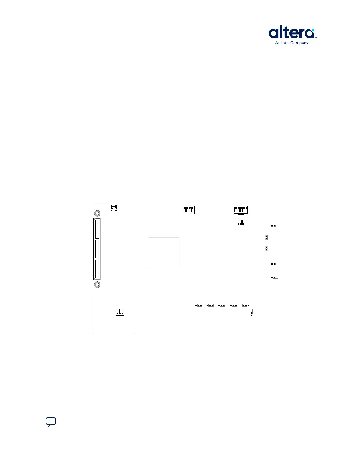
Figure 5. Switch Locations and Default Settings for Power Solution 2 Board
0 1 2 3 4
MSEL
SECURITY
FACT LOAD
Si570
CLK125A
CLKSEL0 CLKSEL1 BOOTSEL0 BOOTSEL1 BOOTSEL2
3 2 1 0 3 2 1 0
FPGA HPS
1 2 3 4
1 2 3 4 5 6
ON
ON
SW1
SW3
SW4
J39
JTAG
HPS SEL
JTAG
SEL
J6
J7
OSC1_CLK_SEL
JTAG_MIC_SEL
J13
J16
J26 J28J27 J29 J30
J31
SPI
I2C
SW2
4 3 2 1
ON
SW6
To restore Cyclone V SoC Development Kit (Power Solution 2) board switches to their
factory default settings, perform these steps:
1. Set the DIP switch bank (SW2) to match the SW2 DIP Switch Settings table.
In the following table, ON indicates the switch is to the left according to the board
orientation as shown in the Switch Locations and Default Settings for Power
Solution 2 figure.
3. Development Kit Setup
830285 | 2024.10.07
Send Feedback
Cyclone
®
V SoC Development Kit User Guide
15