3.2.2. Restoring the Default Settings for Power Solution 1 Board
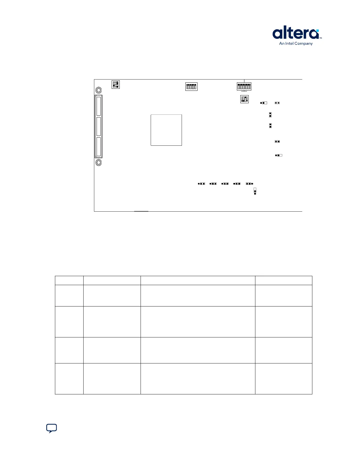
Figure 6. Switch Locations and Default Settings for Power Solution 1 Board
0 1 2 3 4
MSEL
SECURITY
FACT LOAD
Si570
CLK125A
CLKSEL0 CLKSEL1 BOOTSEL0 BOOTSEL1 BOOTSEL2
3 2 1 0 3 2 1 0
FPGA HPS
1 2 3 4
1 2 3 4 5 6
ON
ON
SW1
SW3
SW4
J5 J39
9V
JTAG
HPS SEL
JTAG
SEL
J6
J7
OSC1_CLK_SEL
JTAG_MIC_SEL
J13
J16
J26 J28J27 J29 J30
J31
SPI
I2C
SW2
To restore the Cyclone V SoC Development Kit (Power Solution 1) board switches to
their factory default settings, perform these steps:
1. Set the DIP switch bank (SW2) to match the SW2 DIP Switch Settings table.
In the following table, ON indicates the switch is to the left according to the board
orientation as shown in the Switch Locations and Default Settings for Power
Solution 1 figure.
Table 8. SW2 DIP Switch Settings
Switch Board Label Function Default Position
1 CLK125A Switch 1 has the following options:
• ON (0)—Onboard oscillator is disabled.
• OFF (1)—Onboard oscillator is enabled.
OFF
2 Si570 Switch 2 has the following options:
• ON (0)—Onboard programmable oscillator is
enabled.
• OFF (1)—Onboard programmable oscillator is
disabled.
ON
3 FACT LOAD Switch 4 has the following options:
• ON (0)—Load the factory design starting at
0x20000 at power up.
• OFF (1)—Parallel flash loader (PFL) disabled.
OFF
4 Security Switch 4 has the following options:
• ON (0)—Onboard Intel FPGA Download Cable II
sends FACTORY command at power up.
• OFF (1)—Onboard Intel FPGA Download Cable II
does not send FACTORY command at power up.
OFF
2. Set the DIP switch bank (SW3) to match the SW3 DIP Switch Settings table.
3. Development Kit Setup
830285 | 2024.10.07
Send Feedback
Cyclone
®
V SoC Development Kit User Guide
19